AMD Navi 31 GPU Block Diagram Allegedly Leaked Detailing 3GHz Radeon Beast

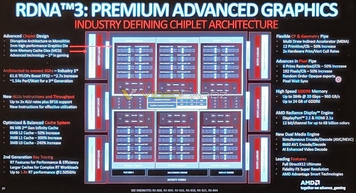
That's not just according to the report we told you about on Saturday, where a reporter let slip that AMD was targeting 3 GHz with Navi 31, but also to a new slide leaked by Videocardz. The picture, which we'll reproduce below, seems to have been taken during an AMD presentation, and it clearly shows a diagram of the Navi 31 GPU, which is the biggest RDNA 3 graphics processor.
Image: Videocardz
It would be, for sure, if it's true. We don't actually know yet what kind of clock rates the Radeon RX 7900 XTX can hit under boost—especially on partner cards that may have an increased power limit and improved power delivery. However, it's rather telling to us that AMD made no public claims about anything to do with "3 GHz" in its presentation. Whether those remarks were cut for time or held back by an anxious lawyer, we may never know.
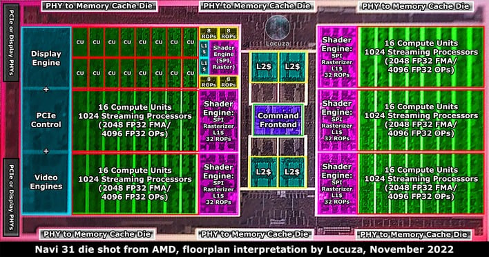
Image: @Locuza_ on Twitter
Twitter user and processor layout enthusiast @Locuza_ has also done one of his trademark annotated die shots for RDNA 3's GCD. If you'll recall, AMD's RDNA 3 GPUs are the first to be designed with a chiplet architecture that splits the graphics processing and compute functions from the memory controllers and cache. Those are on separate dice, which allows them to be manufactured on older processes, since they don't need the ultra-high-density manufacturing that compute functions do. This annotated die shot is only the Graphics and Compute Die, or GCD.


