NVIDIA H100 Hopper GPU With 80GB HBM3 Gets Pictured And It's A Beast

Until today, we had only seen renders of the new part. A few folks had been allowed to lay eyes on the hallowed silicon, but it wasn't until now that NVIDIA allowed anyone outside of its halls to share a few snapshots of H100. The pictures in question come from the boys over at ServeTheHome, a site focused on server and enterprise-class hardware.

Image: ServeTheHome
SXM5 is the latest form factor from NVIDIA for these kinds of parts. It uses a proprietary mezzanine-style connector on the bottom to interface with its host system. Apparently, SXM5 uses a new style of mezzanine connector, too. The overwhelming majority of the SXM5's module is taken up not by the H100 package itself—even as large as it is—but indeed by the monstrous power delivery mechanism for the chip, which NVIDIA says can draw up to 700 watts.
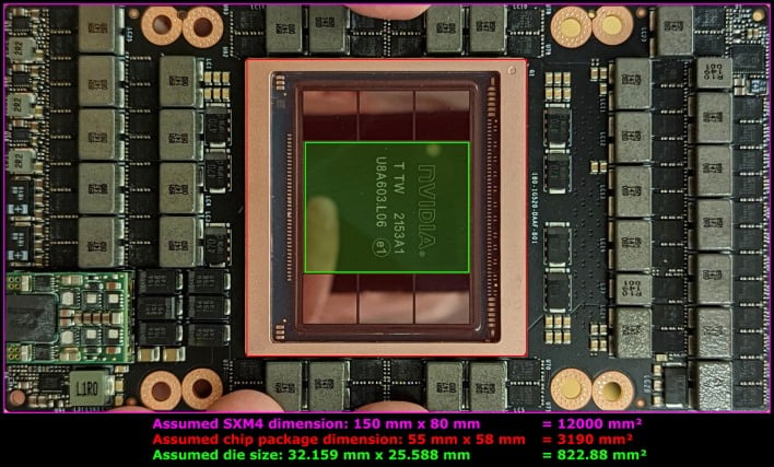
That puts Hopper right in the same region with the Volta V100 die (815 mm²) and the Ampere A100 die (828 mm²) as some of the largest microprocessors ever created. However, Hopper is supposed to be much faster than those two parts, thanks to architectural advancements, bleeding-edge 4nm fabrication, and that crazy 700W power limit. We wrote at length about H100 when NVIDIA announced it; you can read more about it over here.
Images in this post owned by ServeTheHome.