IBM Debuts World's First 2nm Nanonsheet Chips In Critical Semiconductor Breakthrough
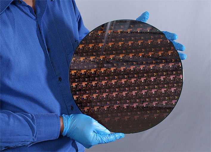
IBM is laying claim to the first chip manufactured on a 2-nanometer manufacturing node, calling it a breakthrough in semiconductor design. To put that into perspective, 2nm is smaller than the width of a single strand of human DNA. Meanwhile, the chip itself is about the size of a human fingernail and is crammed with 50 billion transistors.
"The IBM innovation reflected in this new 2nm chip is essential to the entire semiconductor and IT industry," said Darío Gil, SVP and Director of IBM Research. "It is the product of IBM's approach of taking on hard tech challenges and a demonstration of how breakthroughs can result from sustained investments and a collaborative R&D ecosystem approach."
This sounds pretty wild when you consider Intel is really just getting its feet wet in its 10nm node, and AMD is sourcing 7nm silicon from TSMC, its manufacturing partner. However, it is important to note that comparing nodes from different architectures and chip designs is far more complex than what the node size is labeled as being.
Nevertheless, this is still an impressive achievement on IBM's part. What IBM considers to be a human fingernail width is 150 square millimeters, according to what it told Dr. Ian Cutress at Anandtech, so we're looking at a transistor density of 333 million transistors per square millimeter.
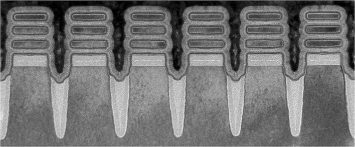
How does that compare to other chip makers? Well, Intel's 10nm node packs 100.76 million transistors per square millimeter, while TSMC's 7nm node is at 91.2 million transistors per square millimeter. IBM's 2nm node leverages a triple-stack Gate-All-Around (GAA) design, as can be seen in the image above, with a cell width of 40nm.
Generally speaking, packing more transistors per chip can make them smaller and faster, and more power efficient. In this case, IBM claims its 2nm nanosheet technology can achieve 45 percent higher performance compared to today's most advanced 7nm chips, or consume 75 percent less power at the same level of performance.
What does this mean for consumers? According to IBM, possible implications include a quadrupling of battery life in cell phones (imagine only have to charge your phone once every four days or thereabouts, rather than daily), faster object detection and reaction time in autonomous vehicles, speedier laptops, and so forth.
Exciting stuff for sure, despite there being no mention of when this breakthrough technology will find its way into consumer electronics.


