IBM, GlobalFoundries And Samsung Partner To Develop World’s First 5nm Nanosheet Process For 30 Billion Transistor Chips
IBM has teamed up with semiconductor equipment suppliers and manufacturing bigwigs GlobalFoundries and Samsung to develop a new process for building silicon nanosheet transistors. This new process paves a path to 5-nanometer, with the subsequent "fingernail-sized" chips packing a staggering 30 billion transistors inside. Hooray for keeping Moore's Law intact.
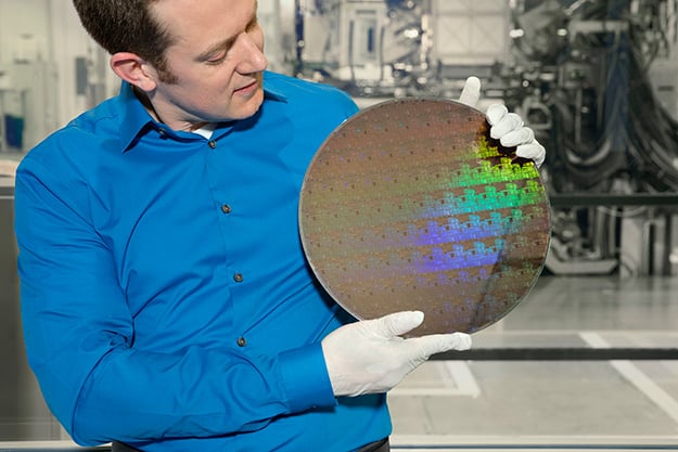
Image Source: Connie Zhou via IBM
"This announcement is the latest example of the world-class research that continues to emerge from our groundbreaking public-private partnership in New York," said Gary Patton, CTO and Head of Worldwide R&D at GlobalFoundries. "As we make progress toward commercializing 7nm in 2018 at our Fab 8 manufacturing facility, we are actively pursuing next-generation technologies at 5nm and beyond to maintain technology leadership and enable our customers to produce a smaller, faster, and more cost efficient generation of semiconductors."
Shrinking the manufacturing process down from 10nm (what Intel is using for Cannonlake) to 5nm provides up to a 40 percent performance enhancement at fixed power, or 75 percent power savings at matched performance. There are real-world benefits in either direction. If going raw performance route, these 5nm chips can help accelerate cognitive computing efforts, which is a red hot field now. And if looking to save power, these chips can lead to more capable Internet of Things (IoT) devices. IBM also says that power savings could lead to batteries in smartphones and other products that could last up to three times longer than today's devices.

Image Source: Connie Zhou via IBM
"For business and society to meet the demands of cognitive and cloud computing in the coming years, advancement in semiconductor technology is essential," said Arvind Krishna, senior vice president, Hybrid Cloud, and director, IBM Research. "That’s why IBM aggressively pursues new and different architectures and materials that push the limits of this industry, and brings them to market in technologies like mainframes and our cognitive systems."
Scientists achieved the breakthrough by using stacks of silicon nanosheets as the device structure of the transistor. This is a deviation from the standard FinFET architecture, which has served as the blueprint for the semiconductor industry up through 7nm. IBM has been researching this method for a decade, though this is the first time it has been able to demonstrate the feasibility of designing and fabricating nanosheet devices with electrical properties superior to FinFET.
Image Source: Connie Zhou via IBM
"This announcement is the latest example of the world-class research that continues to emerge from our groundbreaking public-private partnership in New York," said Gary Patton, CTO and Head of Worldwide R&D at GlobalFoundries. "As we make progress toward commercializing 7nm in 2018 at our Fab 8 manufacturing facility, we are actively pursuing next-generation technologies at 5nm and beyond to maintain technology leadership and enable our customers to produce a smaller, faster, and more cost efficient generation of semiconductors."
Shrinking the manufacturing process down from 10nm (what Intel is using for Cannonlake) to 5nm provides up to a 40 percent performance enhancement at fixed power, or 75 percent power savings at matched performance. There are real-world benefits in either direction. If going raw performance route, these 5nm chips can help accelerate cognitive computing efforts, which is a red hot field now. And if looking to save power, these chips can lead to more capable Internet of Things (IoT) devices. IBM also says that power savings could lead to batteries in smartphones and other products that could last up to three times longer than today's devices.

Image Source: Connie Zhou via IBM
"For business and society to meet the demands of cognitive and cloud computing in the coming years, advancement in semiconductor technology is essential," said Arvind Krishna, senior vice president, Hybrid Cloud, and director, IBM Research. "That’s why IBM aggressively pursues new and different architectures and materials that push the limits of this industry, and brings them to market in technologies like mainframes and our cognitive systems."
Scientists achieved the breakthrough by using stacks of silicon nanosheets as the device structure of the transistor. This is a deviation from the standard FinFET architecture, which has served as the blueprint for the semiconductor industry up through 7nm. IBM has been researching this method for a decade, though this is the first time it has been able to demonstrate the feasibility of designing and fabricating nanosheet devices with electrical properties superior to FinFET.