Intel's Massive $3B Oregon Chip Fab Expansion Is Open To Accelerate Its IDM 2.0 Strategy
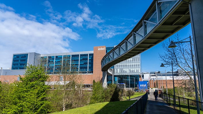
Intel today cut the ribbon on a massive expansion to its leading-edge D1X factory located in Hillsboro, Oregon. It also announced a new name for the nearly 500-acre campus. Previously called Ronler Acres, this cutting edge development chip fab has now been anointed Gordon Moore Park at Ronler Acres in honor of Intel co-founder Gordon Moore and his 1965 prediction that famously became known as Moore's Law.
Moore's Law has been a driving force at Intel. In simple terms, it's essentially an observation that the number of transistors in a microchip will approximately double ever two years, and from Intel's vantage point, Moore's forecast set the pace for silicon technology advances over the past several decades (more than 50 years at this point).
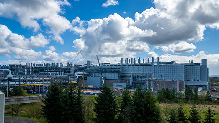
Intel's D1X expansion adds nearly 270,000 square feet of clean room space
That continues today with Intel CEO Pat Gelsinger having outlined an aggressive IDM 2.0 strategy to put the company back on track in terms of Intel's leadership in fab process technologies and innovation.
"Since its founding, Intel has been devoted to relentlessly advancing Moore’s Law. This new factory space
will bolster our ability to deliver the accelerated process roadmap required to support our bold IDM 2.0
strategy," Gelsinger said.
"Oregon is the longtime heart of our global semiconductor R&D, and I can think of no better way
to honor Gordon Moore’s legacy than by bestowing his name on this campus, which, like him, has had
such a tremendous role in advancing our industry," he added.

The factory expansion is called Mod3 and it adds 270,000 square feet of clean room space to the existing fab site. It will be used to develop next-generation silicon process technologies, including RibbonFET (the first new transistor architecture in more than a decade), PowerVIA (a new backside power delivery method), and the first use of High-NA EUV (Extreme Ultraviolet) lithography.

These are technologies that will help drive Intel in to the "angstrom era" of semiconductor design, starting with the Intel 20A process node. Intel also notes that at any given time, its D1X site is home to multiple logic process technologies in various states of the development cycle.
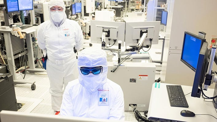
This $3 billion investment goes into a site that contains the largest concentration of facilities and talent in the world, Intel says. D1X is Intel's largest R&D site and home to nearly 22,000 employees across four campuses in Hillsboro, which is located 20 miles west of Portland. This expansion brings Intel's total investment in Oregon to more than $52 billion to date.
It also follows huge spending commitments in other campuses, such as the $20 billion mega-site in Ohio and $88 billion in expansion plans in Europe.