Intel and Numonyx Unveil Stacked, Cross Point Phase Change Memory
Intel and Numonyx held a press conference earlier today to discuss a phase change memory (PCM) breakthrough many years in the making. The companies have been jointly exploring the possibilities of multi-layered or stacked PCM cell arrays, and have finally been able to demonstrate a 64Mb test chip that has the ability.
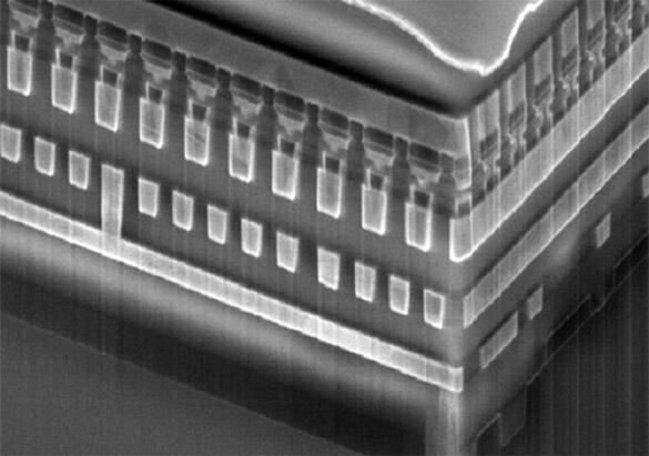
These vertically integrated memory cells, dubbed PCMS (phase change memory and switch), will be comprised of one PCM element layered with an Ovonic Threshold Switch (OTS) in a true cross point array.
Intel and Numonx PCMS, Phase Change Memory and Switch
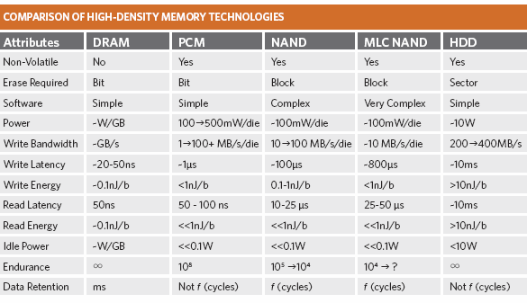
PCM memory uses material state as an identifier, either crystalline or amorphous, to determine the state of a cell (1 or 0) and doesn't require the higher voltages of traditional storage memory, like NAND flash, to function. PCM arrays can be built down to geometries of 5nm or smaller and can alter memory contents at the bit level rather than the block modification necessary with NAND which in-turn can offer lower latency. PCM has DRAM-like features but is also non-volatile and with its stackability, scalability should be much higher than NAND. The companies claim a Moore's Law type of density scaling is possible in future generation storage devices.
The official press release regarding the announcement is posted below...
INTEL AND NUMONYX ACHIEVE RESEARCH MILESTONE WITH STACKED, CROSS POINT PHASE CHANGE MEMORY TECHNOLOGY
New Research Discovery Paves Way for Scalable, Higher Density Phase Change Memory Products
SANTA CLARA, Calif., and GENEVA – Oct. 28, 2009 – Intel Corporation and Numonyx B.V. today announced a key breakthrough in the research of phase change memory (PCM), a new non-volatile memory technology that combines many of the benefits of today's various memory types. For the first time, researchers have demonstrated a 64Mb test chip that enables the ability to stack, or place, multiple layers of PCM arrays within a single die. These findings pave the way for building memory devices with greater capacity, lower power consumption and optimal space savings for random access non-volatile memory and storage applications.
The achievements are a result of an ongoing joint research program between Numonyx and Intel that has been focusing on the exploration of multi-layered or stacked PCM cell arrays. Intel and Numonyx researchers are now able to demonstrate a vertically integrated memory cell – called PCMS (phase change memory and switch). PCMS is comprised of one PCM element layered with a newly used Ovonic Threshold Switch (OTS) in a true cross point array. The ability to layer or stack arrays of PCMS provides the scalability to higher memory densities while maintaining the performance characteristics of PCM, a challenge that is becoming increasingly more difficult to maintain with traditional memory technologies.

"We continue to develop the technology pipeline for memories in order to advance the computing platform,” said Al Fazio, Intel Fellow and director, memory technology development. "We are encouraged by this research milestone and see future memory technologies, such as PCMS, as critical for extending the role of memory in computing solutions and in expanding the capabilities for performance and memory scaling.”
"The results are extremely promising,” said Greg Atwood, senior technology fellow at Numonyx. "The results show the potential for higher density, scalable arrays and NAND-like usage models for PCM products in the future. This is important as traditional flash memory technologies face certain physical limits and reliability issues, yet demand for memory continues to rise in everything from mobile phones to data centers.”
Memory cells are built by stacking a storage element and a selector, with several cells creating memory arrays. Intel and Numonyx researchers were able to deploy a thin film, two-terminal OTS as the selector, matching the physical and electrical properties for PCM scaling. With the compatibility of thin-film PCMS, multiple layers of cross point memory arrays are now possible. Once integrated together and embedded in a true cross point array, layered arrays are combined with CMOS circuits for decoding, sensing and logic functions.
More information about the memory cell, cross point array, experiment and results will be published in a joint paper titled "A Stackable Cross Point Phase Change Memory,” and will be presented at the 2009 International Electron Devices Meeting in Baltimore, Md., on Dec. 9. The paper is co-authored by Intel and Numonyx technologists and will be presented by DerChang Kau, Intel senior principal engineer.