Intel Foundry Reveals New Roadmap Details And Partnerships For The Age Of AI

In fact, Intel Foundry is claiming it is the “the world’s first systems foundry for the AI era, delivering leadership in technology, resiliency and sustainability.” To that end, the company announced updates to its process roadmap, along with plans to fortify its supply chains, and consistently improve its sustainability over the next two decades. According to the company, the plan is for Intel to be the industry’s most sustainable foundry.
Last year the company estimated that it used 99% renewable electricity in its factories, and today it disclosed its commitment to achieving 100% renewable electricity worldwide, net-positive water, and zero waste to landfills by 2030. Intel Foundry also plans to achieve net-zero Scope 1 and Scope 2 Greenhouse Gas emissions by 2040 and net-zero upstream Scope 3 emissions by 2050.
Accelerating Execution To Achieve Process Leadership
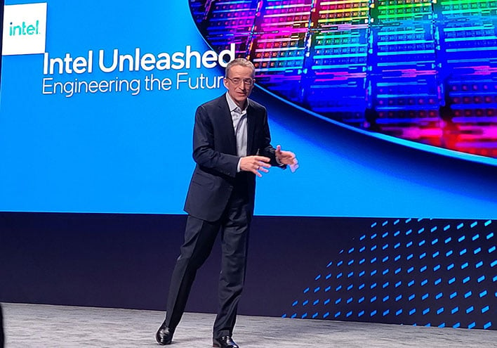
Since Pat Gelsinger took the helm of Intel, the company has been laser-focused on regaining its process leadership position, and announced plans to launch five nodes in four years. CEO Pat Gelsinger and Stu Pann, SVP, GM, Intel Foundry Services, not only reiterated the company’s commitment to achieve that goal – which appears to be on-track – but it further expanded on the roadmap and explained how it plans to be the world’s second largest foundry by 2030.
In the nearer term, Intel Foundry will deliver the industry’s first backside power solution and the company believes it will regain process leadership with Intel 18A in 2025. Customer can already design products for 18A now, with full production scheduled for Q2. Intel also highlighted that it's next-gen Clearwater Forest 288-core Xeon (the follow-up to Sierra Forest), has already taped out.
Intel’s latest process roadmap (above), which it disclosed at the event, adds Intel 14A to the company’s node plan, along with a number of additional node updates and enhancements. Intel's new 14A node will feature High-NA EUV lithography and will initially be developed in Oregon. The new roadmap includes node advancements for Intel 3, Intel 18A, and Intel 14A process technologies, that include Intel 3-T, which will feature through-silicon vias for 3D chip stacking, 18A-P, and 16-E, among others. The “P”, “T”, and “E” designations all represent specialized node enhancements, which will bring performance improvements, feature additions, or both. The “P” (performance) designation signifies approximate >5% - 10% performance improvements, while the “E” designation signifies new features or devices, and potential performance improvements of less than 5%. Performance improvements greater than 10% may be designated as a new node.
These node advancements are designed to allow customers to design and develop products tailored to their specific needs and timeline. Intel Foundry Services plans a new node every two years, adding enhancements, which the company calls node evolutions, along the way.
Intel Foundry Services: More Than Just Transistors
Intel also announced the addition of Intel Foundry FCBGA 2D+ to its suite of advanced systems assembly and test (ASAT) offerings, which already include FCBGA 2D, EMIB, Foveros and Foveros Direct. Of course, Intel highlighted the readiness of its mature process nodes too, including new 12 nanometer nodes coming by way of its joint development with UMC announced last month.
Intel’s EDA partners Synopsys, Cadence, Siemens, Ansys, Lorentz and Keysight all disclosed tool qualification and IP readiness to enable foundry customers to accelerate chip designs on Intel 18A, in addition to EDA and IP enablement across Intel’s additional node families. In addition plans are being put in place to collaborate on assembly technology and design flows for Intel’s embedded multi-die interconnect bridge (EMIB) 2.5D packaging technology.
Moving forward, it’s clear Intel Foundry will be a key pillar for for Intel and instrumental for adding significant bleeding-edge foundry capacity for the industry as a whole. There are a number of reasons Intel will be investing upwards of $200B in the coming years into IFS, and has formed alliances and partnerships with a myriad of leading players in semiconductors, semiconductor IP, and EDA. Not only will Intel Foundry be a key enabler for partners, but potentially a major profit center for the company as well, all while bringing a significant amount of advanced semiconductor manufacturing capacity back to U.S.


