Intel Stacked Forksheet Transistor Patent Could Keep Moore's Law Going In The Angstrom Era
We've been measuring integrated circuit feature sizes in nanometers for years now, but some folks reading this are probably as old or older than yours truly, who can recall when we first talked about microprocessors being fabricated at the sub-micron feature size. If you don't know, one micron is one micro-meter, or one-thousand nanometers.
We're on the cusp of another measuring unit shift in microprocessor manufacturing within the next few years, and this time it'll be from nanometers to angstroms. One angstrom is equivalent to one-tenth of a nanometer. This unit is most frequently used to measure the breadth of wavelengths of visible light, so these are some tiny transistors, folks.
A lot of people have written ad nauseum about the end of Moore's Law, but Intel isn't ready to see the adage, named after its co-founder Gordon Moore, go just yet. Current CEO and former CTO Pat Gelsinger has said exactly that as recently as this past December.

Before that, in July, the company published slides introducing its renamed fabrication nodes, and while some mis-informed rubes heaped derision on the company for the decision, the most interesting part of that announcement was actually on the opposite end of the slide where Intel says that its next process after Intel 3 will be called Intel 20A.
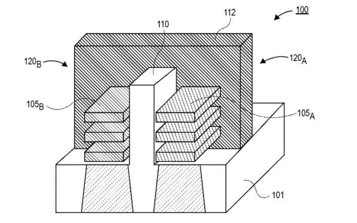
"20A" refers to 20 Angstrom, or 2 nanometers. Intel described its technique for fabricating transistors at that feature size as a technology called RibbonFET, and stated that 18A will come shortly after, with refinements to the design from 20A. What kind of refinements? Well, maybe something like what's described in this new Intel patent that the USPTO just published. Filed on June 26th of 2020, the patent describes a method for fabricating "stacked forksheet transistor devices."
Now, that "forksheet" term sounds familiar. Where have we heard that before? Oh yes—it was in this publication from Belgium's Imec. That document, from 2019, describes a structure that sounds, at least at a surface level, extremely similar to the technique that Intel just patented.
We're not circuit engineers, so we haven't fully digested that entire patent filing just yet. Still, from what we can glean, this approach isn't fundamentally different from what Intel and other fabs are already doing, such as with Big Blue's RibbonFET. Basically, the stacked forksheet approach takes an existing gate-all-around nanosheet and inserts a wall (of dielectric material) between the P-gate and N-gate devices. This allows much tighter spacing between the gates.
Intel's patent makes no claims about performance, scalability, efficiency, or anything else, but Imec's paper is more exciting in that regard. The group claimed back in 2019 to have demonstrated a forksheet device and attained either a 10% speed gain at iso-power or a 24% power reduction at iso-speed when compared to a traditional nanosheet device. Either of these gains come along with a 20% cell area reduction, which improves to 30% for SRAM.
If you ARE an engineer, you can check out the patent over here [PDF].