Intel Unveils New Chip Packaging Tech To Fuel Its Next-Gen Processor Designs
We are in the era of chiplet designs, and given the growing complexity of today's silicon solutions, that is unlikely to change anytime soon. Along those lines, one thing Intel says often gets overlooked is the chip packaging on modern designs. As such, Intel is showcasing a new three-dimensional chip packaging technique that essentially combines Embedded Multi-Die Interconnect (EMIB) and Foveros.
The new packaging technique is called Co-EMIB. It enables the linkage of even more computing performance and capabilities, Intel says, in part by allowing for the interconnection of two or more Foveros elements with essentially the performance of a single chip. It also allows designers to connect analog, memory, and other tiles (chiplets) with high bandwidth, and at low power.
Here's a look at Co-EMIB...
"More than just the final step in the manufacturing process, packaging is becoming a catalyst for product innovation. Advanced packaging techniques allow integration of diverse computing engines across multiple process technologies with performance parameters similar to a single die, but with a platform scope that far exceeds the die-size limit of single-die integration. These technologies will improve product-level performance, power and area while enabling a complete rethinking of system architecture," Intel says.
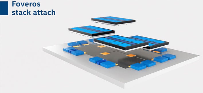
You may recall that EMIB debuted on Kaby Lake-G, a collaborative product between Intel and AMD that paired the former's CPU technology with the latter's Radeon graphics. Foveros, meanwhile, was announced late last year. It is a 3D chip stacking technology that will debut in Lakefield processors later this year.

Chip packaging is the final step in CPU assembly, though also a critical one, as it pertains to future innovations. Co-EMIB paves the way for stacked 3D chips to communicate with one another through a high speed interface. This can be done both horizontally and vertically with something called through-silicon vias (TSVs), available in Intel's Omni-Directional Interconnect (ODI) tech. This allows for power delivery to the top die directly from the package substrate, Intel says.
"Much larger than traditional TSVs, the large vias have lower resistance, providing more robust power delivery simultaneously with higher bandwidth and lower latency enabled through stacking. At the same time, this approach reduces the number of TSVs required in the base die, freeing up more area for active transistors and optimizing die size," Intel explains.
Intel also announced a new die-to-die interfaced called MDIO. According to PCWorld, Intel noted at Semicon West that MDIO will provide a 5.4Gbps pin speed, and will be available in 2020.
The bottom line here is that Intel is putting the literal building blocks in place for future designs. What those end up being (beyond what we already know is in the pipeline), only time will tell.