Toshiba Spin-Off Kioxia Develops 3D Semicircular Flash Memory That Could Supplant QLC NAND
A company called Kioxia (spun out of Toshiba) has developed an interesting technology that could potentially pave a path beyond today's quad-level cell (QLC) NAND flash memory chips, into the next-generation of penta-level cell (PLC) parts. It's a breakthrough of sorts, in that it's the world's first three-dimensional semicircular split-gate flash memory cell structure.
The name for this tech is Twin BiCS flash. There's a ton of technobabble in the press announcement, but the short version is, Kioxia developed a novel way of packing smaller cells to increase memory density beyond what is possible with today's QLC NAND flash memory technology.
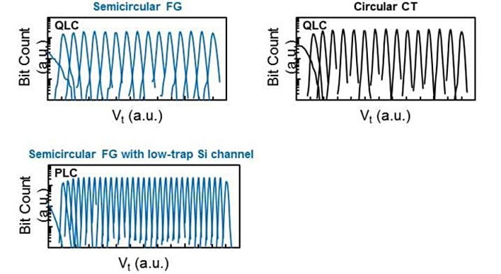
"Twin BiCS flash achieves superior program slope and a larger program/erase window at a much smaller cell size compared to conventional circular Charge Trap (CT) cells. These attributes make this new cell design a promising candidate to surpass four bits per cell (QLC) for significantly higher memory density and fewer stacking layers," Kioxia explains.
Kioxia has effectively found an end-around to stacking more layers on top of each other, as current solutions have already scaled to 128 layers. Instead, the semicircular flash memory cell structure Kioxia developed splits the gate electrode in a conventional circular cell to reduce the overall cell size. This in turn enables higher density memory at a lower number of cell layers.
"In this split-gate cell design, the circular control gate is symmetrically divided into two semicircular gates to take advantage of the strong improvement in the program/erase dynamics," Kioxia says.
Kioxia contends that this is the way to go as memory technology soars past 100 layers. Time will tell, though, as it will be a few years before this technology moves to the implementation stage.