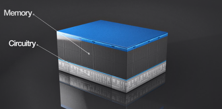
Micron Ships World's First 176-Layer NAND With Huge Gains In Performance And Storage Density

With the move to a 176-layer design, Micron says that both read and write latency has been improved in excess of 35 percent, while offering a die size that is 30 percent smaller than its competitive set. In addition, the company is quoting maximum data rates of up to 1,600 MT/s using the ONFI bus, which is a 33 percent improvement over current-generation 96-layer and 128-layer solutions. And in case you were wondering, this is a triple-level cell 3D NAND design.
Given how prevalent NAND flash is in today's climate, Micron is envisioning that its chips will be found in a wide variety of products from smartphones, to consoles, to drones, to automotive infotainment systems, to solid state drive (SSDs) that will be used for client and data center applications (including the company’s consumer-level Crucial SSDs).
“Micron’s 176-layer NAND sets a new bar for the industry, with a layer count that is almost 40% higher than our nearest competitor’s,” said Scott DeBoer, executive vice president of technology and products at Micron. “Combined with Micron’s CMOS-under-array architecture, this technology sustains Micron’s industry cost leadership.”
“The rising adoption of 5G and AI is quickly pushing smartphone storage to its limits as consumers look to seamlessly multitask across data-intensive applications,” added Raj Talluri, senior vice present and general manager of Micron’s Mobile Business Unit. “Filling this gap with powerhouse performance in a tight package, our leading-edge 176-layer NAND is equipped to scale with demanding mobile workloads — enabling snappier user experiences across computational photography, graphic-rich gaming, edge computing and beyond.”
Micron Transitioning To Second-Generation 3D Replacement-Gate NAND Technology
Looking ahead to the future of NAND technology, Micron is moving towards next-generation 3D replacement-gate (RG) NAND technology, which promises unmatched advances in power efficiency, performance, and storage capacity. Micron is adopting RG because traditional 3D NAND is starting to hit limitations with respect to cell-to-cell capacity coupling, which is a cell characteristic that results in slower programing times, which in turns leads to reduced performance.
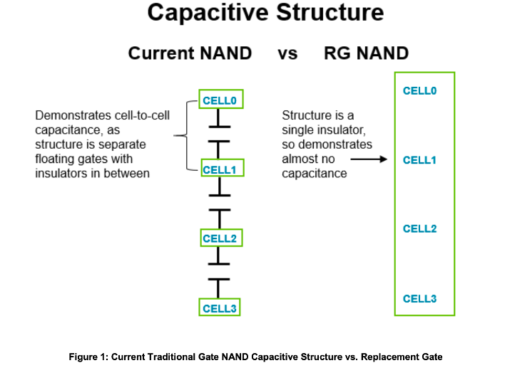
3D RG NAND gets around this by using a nonconductive layer of silicon nitride, which in effect functions as a NAND storage cell that traps electrical chargers. The layer surrounds the control gate, insulating the stored charge to reduce the cell-to-cell capacity coupling that affects traditional NAND structures.
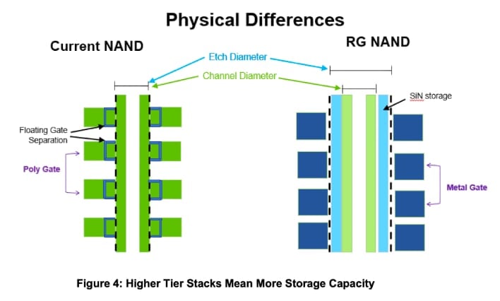
Micron claims that by switching from traditional 3D NAND to 3D RG NAND; read, write, and erase operation scan be performed up to twice as fast. There is also a resultant reduction in electrical field duration within the circuits, which in turn increases endurance (without having an adverse effect on power efficiency and performance). If that wasn't enough, overall life of a NAND cell is increased 3D RG NAND has a wider pillar etch that allows for higher tier stakes to further boost storage capacities going forward.