Micron Unveils 232 Layer NAND Paving The Way For Faster And Bigger Capacity SSDs
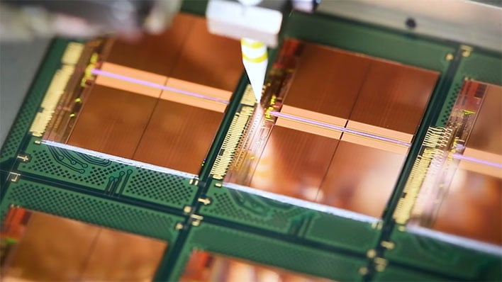
Micron delivered some pretty big news today, saying it has begun volume production of the industry's first 232-layer triple-level cell (TLC) NAND flash memory chips with huge gains in area density, capacity, energy efficiency, and performance. In short, it's an improvement over 176-layer NAND in practically every conceivable way.
Or to put it in Micron's own words, this is a "watershed moment for storage innovation," serving as the first proof that it can scale 3D NAND flash to more than 200 layers in volume production. Not that it was an easy achievement by any stretch, but an important one.
"This groundbreaking technology required extensive innovation, including advanced process capabilities to create high aspect ratio structures, novel materials advancements and leading-edge design enhancements that build on our market-leading 176-layer NAND technology," said Scott DeBoer, executive vice president of technology and products at Micron.

Today's packaging technologies are increasingly reliant on stacking solutions. Micron likens this to building in an expensive, overcrowded city. Instead of expanding outward, which is not a viable or cost effective way to increase density, taller buildings take advantage of vertical space to add more levels and units in the same compact footprint.
It's an oversimplified analogy, but Micron's 3D NAND takes the same general approach. According to Micron, its 232-layer solution enables the industry fastest NAND I/O speed at 2.4GB/s, which is 50 percent faster than the previous generation 176-layer solution. It also delivers up to 100 percent higher write bandwidth and more than 75 percent higher read bandwidth per die, the company claims.
"In addition, 232-layer NAND introduces the world’s first six-plane TLC production NAND.3 It has the most planes per die of any TLC flash3 and features independent read capability in each plane," Micron adds.
According to Micron, utilizing a six-plane architecture means fewer collisions between write and read commands, which in turn delivers critical system-level quality-of-service (QoS) improvements.
There are also benefits on capacity side of the equation. Leveraging a 232-layer design has allowed Micron for the first time to achieve a 1-terabit (Tb) TLC die, which is double that of its 176-layer design. It's touting the highest TLC density per square millimeter (14.6 Gb/mm2) ever made, with an area density that is anywhere from 35-100 percent greater than competing TLC products currently available.
What this all means is that drive makers will be able to deliver faster and more capacious SSDs, and just in time for a push into PCIe 5.0 territory. It sounds like Micron will give its own Crucial brand first dibs, but says to expect additional product and availability announcements.