NVIDIA GeForce MX350 And MX330 Mobile Pascal GPUs Shine In Benchmark Leaks

NVIDIA is gearing up to launch a couple of entry-level mobile GPUs, namely the GeForce MX350 and GeForce MX330, to take on integrated solutions from AMD and Intel. According to NVIDIA, the GeForce MX350 offers up to 2.5X faster performance while the GeForce MX330 is up to 2X faster compared to the "latest and best integrated graphics for photo editing, video editing, and gaming." Are they really, though? It's too early to tell, but some leaked benchmarks give us an early look at performance.
While the benchmark runs are unofficial, these GPUs do exist—NVIDIA has put up separate product pages for each GPU. The product pages only reveal a few basic details, such as GDDR5 memory support and checkmarks for technologies such as Optimus and PCI Express 3.0. Clockspeeds and everything else is still under lock and key. Well, officially.
According to Notebookcheck, both GPUs are actually based on NVIDIA's previous generation Pascal architecture, and not Turing. However, in a separate article, the site also says it heard from its sources that NVIDIA plans to launch a Turing-based MX GPU sometime later this year, to duke it out with Intel's discrete Xe DG1.
Let's start with the leaked specifications...
- GeForce MX350 (N17S-G5): 16nm, 640 CUDA cores, 1,354MHz base clock, 1,468MHz boost clock, GDDR5 memory, 64-bit memory bus, 25W TDP
- GeForce MX330 (N17S-G3-A1): 16nm, 384 CUDA cores, 1,531MHz base clock, 1,594MHz boost clock, GDDR5 memory, 64-bit memory bus, 25W TDP
There has also been chatter of a 15W version of the GeForce MX350 with slower 746MHz base and 937MHz boost clocks.
Compared to the MX200 series, the lower end GeForce MX330 essentially looks like a rebranded GeForce MX250 (25W version). It has the same number of CUDA cores and memory configuration, and both are built around Pascal. The GeForce MX330 just sports slighter higher clocks—1,531MHz (base) and 1,594MHz (boost), versus 1,518MHz (base) and 1,582MHz (boost).
The GeForce MX350, meanwhile, is based on the same GP107 GPU found in NVIDIA's GeForce GTX 1050. However, it has a narrower memory bus (64-bit versus 128-bit) and a lower TDP (25W versus 75W).
Leaked NVIDIA GeForce MX350 And GeForce MX550 Performance Benchmarks
What does this all boil down to in terms of actual performance? In the 3DMark (Time Spy and Fire Strike), the higher end GeForce MX350 settles in somewhere between a GeForce GTX 960M and a GeForce GTX 1050. Have a look...
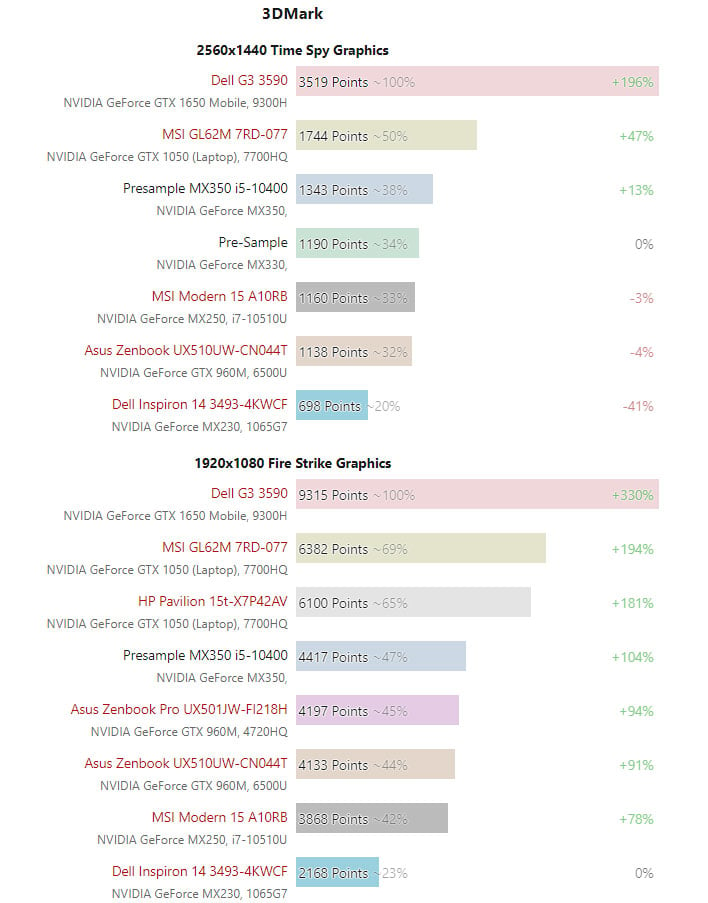
Compared to the previous generation GeForce MX250, the upcoming GeForce MX350 is quite a bit faster, as we would expect when looking at the specifications. At the same time, these are lower end discrete GPUs that, for gaming, will be best served at lower settings and with less demanding games.
In a separate benchmark leak, Twitter user _rogame posted a chart plucked from a Chinese-language website that has already reviewed the GeForce MX350.
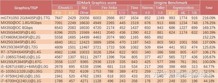
It's more of the same, really, but with a wider assortment of benchmarks (Heaven 4.0, Valley 1.0, and a few others thrown into the mix).
We find it interesting that these parts exist (and presumably will soon be on the market), if a Turing-based MX GPU is right around the corner. This could be a case of NVIDIA finding ways to sell off older inventories, with new product names and slightly altered specifications. Whatever the case might be, the entry-level graphics market is going to get even more crowded this year.