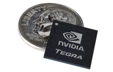
NVIDIA Launches TEGRA System-On-a-Chip Designs
Back in February of this year, NVIDIA announced their APX 2500 application processor. In the official announcement, NVIDIA described the product as a "breakthrough applications processor that enables intuitive 3D user interfaces and engaging high-definition video on connected Windows Mobile phones." -- a tall order to be sure. At the time, we got a chance to play with the APX 2500 development platform and saw the unit's UI first hand. We even saw Quake III running on the device, which brought back memories of the thousands of timedemo runs we've endured over the years, while producing numerous, CPU, GPU, and motherboard related articles. Although NVIDIA didn't disclose any design wins in our meeting, seeing the device in action left us feeling that smartphone and portable navigation device manufacturers would be all over APX 2500. And there were a few "off the record" comments during our meeting that reinforced this feeling.


NVIDIA's APX / TEGRA Development Platform
NVIDIA's Tegra procesor is a relatively tiny piece of silicon considering it is being touted as a "system on a chip". The reference PCB shows a TEGRA processor in the center, surrounded by a couple of Samsung DRAM chips and an 8GB SAMSUNG moviNAND piece of flash memory. The Samsung moviNAND combines high-density MLC NAND flash with an MMC controller in a single chip. The actual development platform device looks much like the one designed for the APX 2500, and resembles many current portable navigation units. Also note the multitude of output and ports on the TEGRA development platform.

NVIDIA TEGRA High-Level Overview
NVIDIA's TEGRA application processor features an ARM11 processor core with a GeForce GPU, and dedicated image and HD video processing engines. The integrated GeForce GPU features programmable pixel shaders and support for OpenGL ES 2.0 and D3D Mobile. TEGRA processing units are coupled to a low-power DDR memory interface, display outputs - including HDMI and they support both NAND and NOR flash memory for storage. What's perhaps most impressive is that, at idle, the chips consume less than 100 mW.

If we compare the features and clock speeds of the TEGRA 600 and 650 to the APX 2500, it becomes clear that the chips are quite similar. The only totally "new" feature to TEGRA is support for IDE. But the new TEGRA chips also offer support for higher primary LCD resolutions and the TEGRA 650 can decode video at up to 1080P (@ 24 FPS), while the others are limited to 720P (@ 30 FPS).
NVIDIA has worked closely with Microsoft during the development of the APX 2500 and TEGRA application processors, so you can expect some next-gen smartphones running Windows Mobile and various mobile internet devices (MIDs) to be based on them. We also suspect some portable navigation devices will leverage the technology for its relatively high-performance (in the mobile space) 3D graphics support.
For an idea of what NVIDIA has in mind for TEGRA, take a look at the video above. It shows the 3D UI in action.


