NVIDIA GeForce RTX 50 Series May Adopt Chiplet Design With The Blackwell GPU Arch
So when's NVIDIA going multi-chip? Apparently, with its next generation of GPUs. According to regular and reasonably-reliable leaker kopite7kimi, NVIDIA's GB100 GPU, the successor to the Hopper H100 datacenter part, will be fabricated using chiplets in some way. He doesn't elaborate on the exact structure, but in a later tweet reply, he floats the idea that GB100 could be created using a pair of GB102 chips.

This isn't a completely revolutionary idea. AMD's already doing the same thing for its Radeon Instinct MI250 and MI250X accelerators, as used in the Frontier supercomputer. NVIDIA hasn't made a peep about using multi-chip modules yet, but it really isn't surprising to hear that the company might do so with its compute-focused datacenter GPUs. Unlike with graphics workloads, you don't necessarily need to maintain perfect synchronization with a compute workload, so doing it across disparate chips is relatively easy.
This multi-chip design may not actually come to NVIDIA's consumer GPUs at all. The leaker is talking about GB100, which is quite different from GB200. You see, an earlier leak from another source seemed to imply that we won't see the first-generation Blackwell architecture on the desktop. Instead, NVIDIA's next consumer parts will supposedly be based on the GB20x family of GPUs. Going by the company's model names, that would mean that they will be a second revision of the Blackwell architecture.
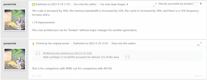
That same source, the user panzerlied over on the Chinese-language Chiphell forums, also posted yesterday about the GeForce RTX 5090. He says that the scale of this chip is increased by 50% over the GeForce RTX 4090, and that it also gains 52% memory bandwidth. Combine that with a supposed 78% increase in cache capacity and a 15% frequency increase, and apparently this results in an overall 70% performance boost.
A gain of 70% over the GeForce RTX 4090 is almost unthinkable. Heck, just the scale difference of 50% is practically unimaginable. The GeForce RTX 4090 is an absolutely gigantic GPU, and leapfrogging it in size by 50% would yield a GPU with nearly 25,000 shader cores. An increase of 52% in memory bandwidth almost assuredly comes with an increase in memory bus width, but it would also require a higher memory transfer rate as well, perhaps utilizing GDDR7 memory.

Yet another recent rumor says that NVIDIA is considering the use of Samsung's 3-nanometer Gate All Around (GAAFET) fabrication process. GAAFETs offer improved density and performance over regular FinFETs, and such an advancement could certainly contribute to making such a powerful GPU. However, most people seem to expect that NVIDIA will stick with TSMC for the new GPUs; kopite7kimi himself remarked that it's "highly unlikely" for NVIDIA to swap over to Samsung for Blackwell.
When are these parts coming? The Blackwell GB100 and other datacenter chips are expected to come some time in 2024. According to an NVIDIA roadmap we saw earlier this year, the consumer parts will then arrive later, in 2025. That'll the first three-year gap NVIDIA's ever had in GPU architectures. We can probably expect some refreshed Ada parts to fill in the gap in the meantime.