AMD’s RDNA 3 Chiplet Patent Details A Cutting-Edge Shader-Optimized Architecture

You see, on a CPU, while there are many shared resources, each task is executed on its own processor core. They're discrete cores running—more-or-less—discrete tasks. That is not the case on a GPU. Generally, on a GPU, huge swaths of the processor (comprising many GPU "cores") will be occupied by a single task, and splitting that across multiple GPU dice without impacting performance is an extremely difficult challenge.
AMD's apparently up to the challenge, though, because the company announced once and for all last month that its upcoming RDNA 3-based "Navi 3" series of graphics processors would make use of chiplets in some form or fashion. As such, we're back to square one: how does AMD plan to split up a GPU into multiple discrete chiplets without affecting performance?
The answer, as it turns out, is apparently "very smart scheduling." That answer comes from a patent filing entered last December, but only published at the end of last month. A community member spotted the publication over at German-language site Computerbase. The patent filing is typically dense with both technical terms and legalese, but the topic of the patent ("Systems and Methods for Distributed Rendering Using Two-Level Binning") is specific enough that we reckon most enthusiasts will get the picture from the name alone.
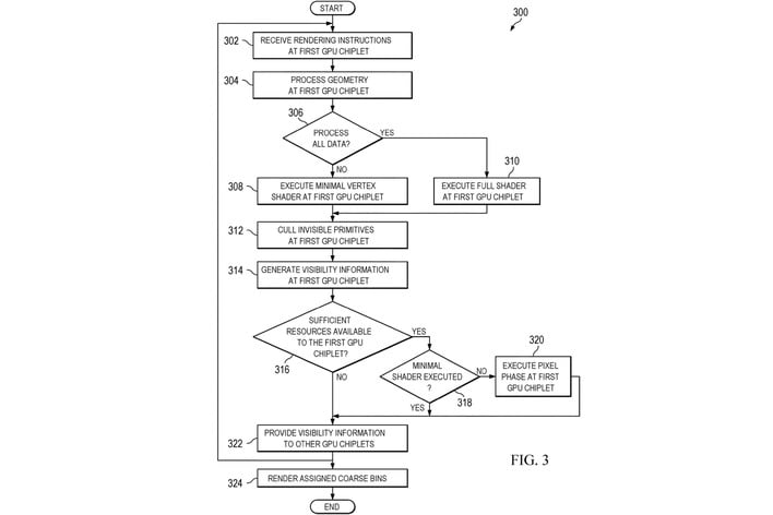
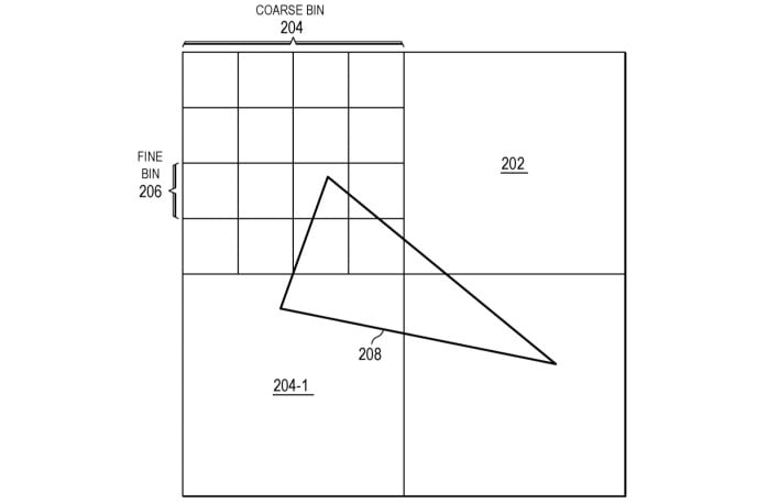
Essentially, as the flowchart from the patent describes it, AMD's GPU will use the first chiplet as a sort of master processor while additional GPU chiplets will be slaved to it. The first GPU will receive the task, and it will make a judgement call whether to handle the task itself—as with older games that simply don't require more GPU compute than the first chip can handle—or to split it up into many bins. Once that's done, if necessary, the task will compute on whichever chiplets were assigned these bins.
All of this sounds like something that will require considerable software optimization, so we hope AMD is on top of things in the driver department. Fortunately, that seems to be the case, at least if the company's recent driver releases are anything to go by.


