Scientists Cook Up A Viable Path To 2nm Semiconductors Using A Modded Microwave Oven

When producing silicon for use in semiconductor fabrication, manufacturers have to dope the silicon with phosphorous and then anneal the mixture to produce a material that can be turned into a working microchip. As chips get ever-smaller, more and more phosphorous is needed, and current methods can't take us past 3nm, where TSMC is currently fabricating the latest chips.
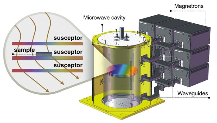
Fortunately, researchers at Cornell University have figured how to heat chips in such a way that they can exceed the natural equilibrium solubility of phosphorous in silicon. The idea first germinated at TSMC, which theorized that microwaves could be used to activate the excess phosphorous, but wasn't able to realize the method using microwave annealers due to "standing waves" mucking up the consistency of the operation.
A diagram from the paper, which you can find here.
TSMC partnered with Cornell University's College of Engineering. Research professor James Hwang took up the task of making the microwave annealer work. Using a modified kitchen microwave, he was able to figure out a way to selectively control where the standing waves occur. That allows for proper activation of the phosphorous dopants without overheating and damaging the silicon's crystal structure.
This research is critical to the development of denser nanosheet transistors, which TSMC has already said that it will use at 2nm. Unlike bleeding-edge research that you read about from time to time, this discovery isn't a decade from market. Hwang says that this approach will allow TSMC and Samsung to move to 2nm (or 20 angstrom) fabrication by the year 2025.