SK Hynix Demos Tallest-Ever 321-Layer 4D NAND To Boost AI And SSD Capacities
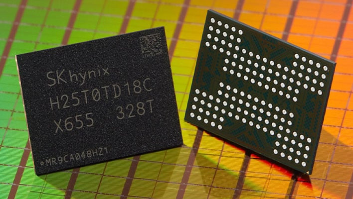
SK hynix is showing off a sample of its 321-layer 1-terabit (Tb) triple-level cell (TLC) "4D" NAND chips, which is notable because it's the first time a chip maker has stacked over 300 layers of NAND flash memory. The demonstration took place this week during the Flash Memory Summit (FMS) 2023 event in Santa Clara, though mass production isn't scheduled until 2025.
While mass production is still a couple of years away, this is an important milestone. Stacking layers upon layers has allowed memory makers to get around the scaling limit of the planar architecture of 2D NAND. This is where 3D NAND comes into play, and somewhat confusingly, 4D NAND. What exactly does that mean?
SK hynix hasn't actually introduced a fourth dimension to NAND. Instead, what it markets as 4D is essentially the same as what its competitors call CMOS under Array (CuA), which entails moving the peripheral circuitry under the cells. The company likens its peri under cell (PUC) approach to that of a blueprint for an apartment building.
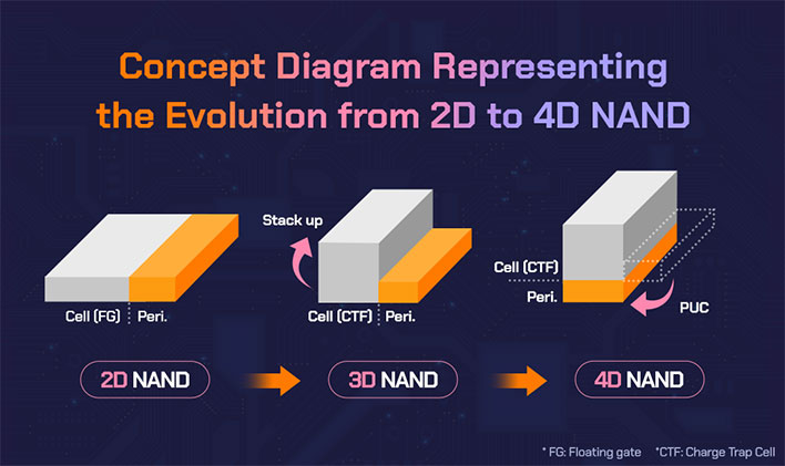
"If an apartment building is a cell, peri is a parking lot, and 3D NAND—where the peripheral circuits are placed at the side—is an outdoor parking area. 4D NAN introduces PUC technology to this, which allows the outdoor parking area to be transformed into an underground parking lot, maximizing space efficiency," SK hynix says of its 4D nomenclature.
Labeling aside, what matters here is that SK hynix is attempting to maintain its density lead after having announced mass production of 238-layer NAND two months ago. Citing "another breakthrough to address stacking limitations," SK hynix has a viable path to surpass 300 layers to help fuel next-generation NAND products such as those optimized for generative AI, UFS 5.0, and PCI Express 6.0.

SK hynix isn't sharing a ton of details at this still-early stage, though it did offer up an interesting nugget—its 321-layer 1Tb TLC NAND boasts a 59% improvement in "productivity" compared to its 238-layer 512Gb NAND, which boils down to being able to extract more NAND capacity from its wafers.
A significant increase in storage density paves the way for more capacious SSDs. Perhaps just as importantly, it could help drive down pricing on bigger SSDs. As things currently stand, 4TB is the upper limit before pricing blasts off into the stratosphere. And of course, SK hynix is playing the AI implications.
"With timely introduction of the high-performance and high-capacity NAND, we will strive to meet the requirements of the AI era and continue to lead innovation.," said Jungdal Choi, head of NAND development at SK hynix.
SK hynix didn't share any specific performance metrics, but did say its 321-layer 1Tb TLC NAND will deliver industry-leading performance when it arrives in earnest.