TSMC's 5nm Node Nearly Doubles The Density Of AMD Ryzen 3000's 7nm Process
In just a few weeks, AMD is expected to roll out its new Ryzen 3000 series of CPUs based on its Zen 2 architecture. These new parts are being built by Taiwan Semiconductor Manufacturing Company (TSMC) on a 7-nanometer node. Looking ahead, however, TSMC is already talking about 6nm and even 5nm, the latter of which will bring improved logic density by 1.8X over 7nm, the company says.
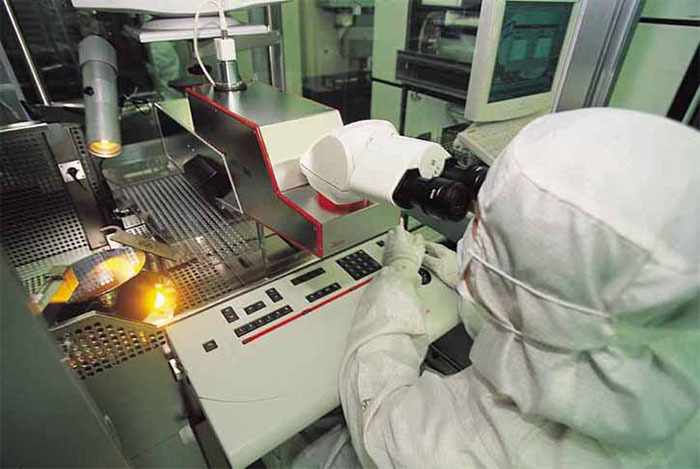
TSMC talked a little bit about its 5nm manufacturing process during a recent earnings call with investors. The company said its 5nm development is "well on track," having entered a phase called "risk production" in the first quarter. It expects a "tape out" in the first half of 2020. That is when designs by clients are finalized for manufacturing.
"With 1.8X logic density and 15 percent
speed gain and (sic) an ARM A72 core compared with 7nm, we believe our N5 technology is the most competitive in the industry.
With the best density, performance, power and the best transistor technology, we expect most of our customers who are using
7nm today will adopt 5nm," TSMC says.
The company also reckons that 5nm will be a "large and long-lasting node." For the average person on the outside looking it, however, all of these nodes can get confusing. That's because TSMC also recently announced a 6nm process, which is not yet in risk production. In other words, TSMC is further ahead on 5nm than it is on 6nm.
How does that make sense? There is no universal standard for measuring and naming nodes. TSMC's 6nm node is really an enhanced version of 7nm—production uses the same equipment, so customers have a comparatively affordable upgrade path to a new node. As it pertains to 6nm, TSMC said it leveraged the new capabilities in extreme ultraviolet (EUV) lithography gained from its N7+ (7nm+) node that is currently in risk production. In a sense, 6nm is sort of like a 7nm++ node.
"We are seeing strong tape-out activities at N7, which include HPC,
IoT and automotive. Meanwhile, our N7+, which adopts EUV for a few critical layers, has already started volume production now. The
yield rate is comparable to N7. We reaffirm N7 and N7+ will contribute more than 25 percent of our wafer revenue in year 2019," TSMC says.
AMD is not TSMC's only customer, though it is one we are very interested in. It's not clear if or when AMD might transition to a 5nm node. As of right now, it's not on the roadmap for Zen. Here's at look at where things stand...
- Zen (Ryzen 1000 series)—14nm
- Zen+ (Ryzen 2000 series)—12nm
- Zen 2 (Ryzen 3000 series)—7nm
- Zen 3 (Ryzen 4000 series?)—7nm+
It's expected that AMD will unveil its new Ryzen 3000 series based on Zen 2 at Computex in June. If AMD sticks to its current roadmap, processors based on its 7nm+ Zen 3 architecture will arrive in 2020. Beyond that, it is anyone's guess what AMD will do.
Circling back to 5nm, TSMC's density claim is based on an ARM processor at 7nm, though it should apply elsewhere. It's interesting to think what AMD could do with that, in terms of Zen 4 if there will be such a thing, or whatever comes after Zen.