Architecture Day 2020: Intel's Tiger Lake, 10nm SuperFin And Xe GPU Arsenal Exposed
Intel Reveals Next-Gen CPU, GPU And Packaging Details In An Aggressive Ready-For-Battle Roadmap

Additional details were revealed regarding Intel’s upcoming Tiger Lake, Willow Cove, Xe Graphics, and hybrid Alder Lake architectures, new 10nm SuperFin technology was revealed, and an array of packaging technologies were discussed as well. There was a ton of information revealed for us to unpack in a relatively short amount of time, bet we’ll do our best to summarize it all for you here.
Enter The Intel 10nm SuperFin
Intel’s struggles bringing up its 10nm node are well-documented at this point, and as it disclosed a few weeks back, its future 7nm process is presenting challenges as well. Intel, however, is claiming that its new 10nm SuperFin technology, which will be used in upcoming Tiger Lake-based products, is “providing performance improvements comparable to a full-node transition,” that is to say the improvements are akin to the benefits the company has seen in the past when moving to newer, more advanced process nodes.That’s a lofty claim, but on the surface the technology does appear to already be paying dividends, should Intel’s performance and power claims regarding Tiger Lake ring true when consumer-ready products arrive in the next few months.
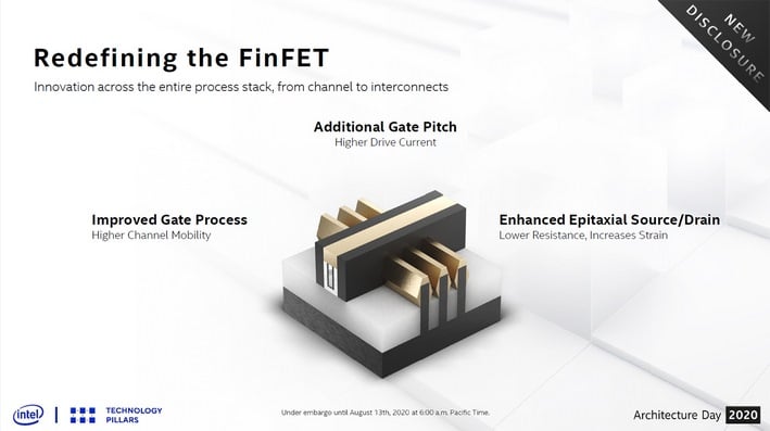
10nm SuperFin technology builds upon Intel’s enhanced FinFET transistors, but adds a new super metal insulator metal capacitor, or Super MIM for short. 10nm SuperFins also have better epitaxial source / drain, an improved gate process and additional gate pitch. The sum total of these enhancements results in better overall transistor performance, lower leakage, and improved power characteristics across a range of voltages. 10nm SuperFins allow for more current through the channel and the improved gate process results in higher drive mobility as well. The higher gate pitch allows the transistor to handle higher drive currents too, which is important in the highest performing circuits on-chip.
Intel is also using a novel thin barrier on 10nm SuperFins, which reportedly reduces resistance by up to 30% and improves overall interconnect performance. According to Intel, 10nm SuperFins can deliver up to a 5x increase in capacitance within the same footprint as previous-gen processes. Intel also notes that the new Hi-K dielectrics being used are arranged in an “industry-first” super lattice structure, that’s only a few angstroms thick.
Tiger Lake And Willow Cove Are On The Horizon And It Looks Bright
Tiger Lake will be the first commercially available product to leverage 10nm SuperFins and Intel is claiming some big performance gains are coming with it. At the heart of Tiger Lake is the semi-new Willow Cove CPU microarchitecture. Willow Cove is heavily based on Sunny Cove, which arrived with Ice Lake. Willow Cove has the same integer and floating-point capabilities as Sunny Cove, but through some architectural enhancements, a redesigned cache structure, and the aforementioned process improvements, Willow Cove is delivering “more than a generational increase in CPU performance,” according to Intel. Willow Cove also has a much wider dynamic range, i.e. it offers significant frequency boosts and power efficiency across the VI curve. Willow Cove essentially runs at much higher frequencies at the same or lower power than Sunny Cove.Willow Cove will feature a larger, non-inclusive cache structure, with 1.25MB L2 per core and a 50% larger Last Level Cache. Willow Cove also features an array of security enhancements with Intel Flow Control Technology, which includes full memory encryption as well.
In addition to Willow Cove-based CPU cores, Tiger Lake features enhanced AI accelerators, updated I/O, and – of course – an Xe-based graphics engine. Tiger Lake’s GNA 2.0 (Gaussian Network Accelerator) is an update to GNA 1.0 that debuted with Ice Lake. GNA engines are a low-power alternative to the CPU for neural network inferencing workloads. Depending on the particular workloads, GNA 2.0 can reduce CPU utilization, and thus power, by up to 20%. Intel notes that the GNA 2.0 engine can offer up 1GigaOps of throughput, per milli-watt, and up to 38GigaOps.
In terms of I/O, Tiger Lake’s got a lot in store. The CPU microarchitecture now features a dual ring bus, and thus a 2x increase in coherent fabric bandwidth, which is commensurate with big increases in memory bandwidth. Initial Tiger Lake-based products will use either LPDDR4 or standard DDR4 memory (validated at up to 4,267MHz or 3,200MHz, respectively), and offer up to 86GB/s of peak bandwidth. Future iterations will use DDR5 memory technology (at up to LP5-5400), which will further reduce power requirements, while increasing bandwidth. Tiger Lake’s memory controller was also reorganized into 8 x 16-bit bundles, with deeper queues, to improve granularity and efficiency.
Tiger Lake also features integrated Thunderbolt 4 and USB 4.0, which are both fully spec compliant according to Intel, along with PCI Express 4.0 connectivity which hangs directly off of the CPU root complex for low latency access of 100ns. Intel’s lack of PCIe 4 has been a sticking point since AMD offers the technology in its desktop and data center processors, so it’s good to see Intel bringing it to mobile with Tiger Lake.
Tiger Lake’s Xe-LP And More Powerful Xe Graphics Architectures
All told, Tiger Lake is reportedly able to deliver more power headroom and significant improvements in absolute performance and performance-per-watt. However, although its Willow Cove CPU cores plays a big part in those improvements, so too does Tiger Lake’s integrated Xe-LP graphics engine.
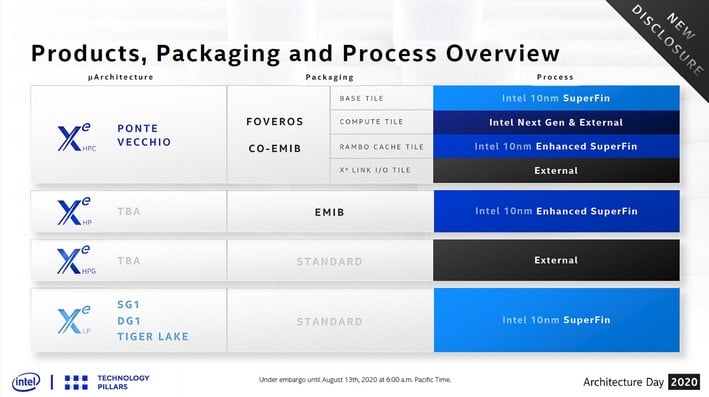
The Xe-LP GPU in Tiger Lake will be equipped with 96 next-gen Execution Units (EUs) with a new L1 data cache and up to 16MB of L3 cache, with an updated media engine, and a new architecture optimized for today’s more taxing graphics, AI and compute workloads. The GPU engine is roughly 1.5x larger than Intel’s Gen 11 graphics, and offers up to 1,536 Flops, up to 48 texels, and up to 24 pixels per clock, through three pipelines. Xe-LP also increases the number of vector lanes from 8 to 16, and it features a more efficient thread controller, in addition to improved color and depth compression algorithms with end-to-end compression, to optimize bandwidth usage.
Intel has already claimed up to a 2x performance improvement over Ice Lake Gen 11 graphics in many workloads and games, that comes by way of its larger engine, in addition to a sizable frequency uplift, and a general redesign of the graphics pipeline.
During the Architecture Day presentations, the company ran a number of demos with Battlefield 1 and GRID, which showed Tiger Lake’s Xe-LP GPU either offering much better performance, or higher image quality at similar performance levels, relative to Gen11 graphics. More importantly, what that means, is that Tiger Lake-based Ultrabooks and other small form factor devices should be able to offer significantly better gaming experiences, in more portable devices and form factors, thanks to Intel Xe-LP Graphics capabilities.
In addition to the next-gen EUs and larger caches, Xe GPUs also features new display and media engines. The display imaging pipeline is fully implemented in hardware now and features a 64-byte wide direct data path from memory to the display, which offers up to 64GB/s of bandwidth in some implementations to support multiple, high-resolution displays. The Intel Xe media engine increases encode / decode performance by approximately 2x and adds AV1 support, HEVC screen content coding support, 4K/8K60 playback, HDR and Dolby Vision support, up to 12-bit BT2020 color, and high refresh rate displays up to 360Hz with adaptive sync.
Xe-HPG - Intel Xe Graphics For Performance Gamers
One of Intel’s fundamental goals with its Xe graphics architecture was to make it highly scalable, from low-power implementations (like the one in Tiger Lake) to high-performance data center applications. Intel notes that Xe is scalable inside the chip, inside the package, and is able to scale up and scale out, which brings us to the Xe-HPG reveal.Intel’s Xe-HPG architecture will target enthusiast gamers. It is a gaming-optimized GPU, which will leverage GDDR6 memory technology (previously disclosed Xe-HP and Xe-HPC GPUs use HBM memory). Intel also announced that Xe-HPG GPU will feature hardware-accelerated Ray Tracing support and that the GPU is already up and running in its labs. There weren’t many details revealed regarding the GPU's configuration, though Intel's Raja Koduri did mention that it would scale up considerably and have many more EUs versus Xe-LP in Tiger Lake. It is also being produced at an external fab, presumably TSMC. In further discussion with Intel execs, we were told that Intel will have Xe graphics for all levels and targets of gaming requirements, from entry-level and midrange to the high end but that Xe-HPG will be the high end GPU. Intel did also reiterate that Xe-HPG is due to ship some time in 2021.
Xe Graphics Software And Features
Intel also detailed that it has revamped its graphics and driver architecture in preparation for Xe, and future GPU generations. The compiler has been improved for optimal performance and the DirectX 11 driver was built from scratch, with a focus on peak performance and local GPU memory usage.There is a new “Instant Game Tuning” option coming, which is essentially a game-specific driver hotfix implementation, that can be pushed to a user’s systems without having to download a complete drive package and do a fresh install. Instant Game Tuning will require a single opt-in from the user on a per game basis.
Xe GPUs will support variable rate shading (VRS Tier 1), game capture and streaming (which leverages the new Xe media engine), and game sharpening will be available as well. Game sharpening is a post-processing technique to boost in-game image quality, similar to what AMD and NVIDIA offer today. Game sharpening will be available as an option in the Intel Graphics Command Center.
Xe GPUs For Servers And Data Centers
Xe-HPG wasn’t the only new GPU disclosed during architecture day. Intel also revealed Xe SG1 for servers. SG1 is an amalgam of four DG1s in a small form factor for data centers, which targets low-latency, high-density Android cloud gaming and video streaming applications. Intel said that SG1 is not in production just yet, but that it will ship to partners later this year.Although we already knew about Xe-HP, Intel did have some additional information to share regarding its high performance Xe GPU for data centers as well. Apparently the company already has Xe-HP silicon back from the fabs and it has successfully powered up. Xe-HP leverages a scalable tile architecture, and can scale from one to four tiles, akin to a multi-die / multicore GPUs. During the Architecture Day presentations, Intel demonstrated Xe-HP transcoding 10 streams of high-quality 4K60 video on a single tile. Another demo showed the compute scalability of Xe-HP across multiple tiles.
Intel is already sampling Xe-HP with key partners and plans to make it available next year.
Intel Data Center Advances: Leveraging All Types Of Compute
While we’re on the subject of data center technologies, we should also mention some information regarding upcoming Xeon Scalable offerings.The first 10nm Ice Lake-based Xeon Scalable processors, which feature total memory encryption, PCIe Gen 4 and eight memory channels, with additional instruction-set architecture to speed up crypto processing, are slated to arrive by the end of 2020.
Beyond the Ice Lake-based Xeons, Sapphire Rapids is Intel’s next-generation family of Xeon Scalable processors. Like Tiger Lake, Sapphire Rapids is based on enhanced SuperFin technology, and as such, should offer better performance and power characteristics. Sapphire Rapids will also support new technologies including DDR5, PCIe Gen 5, Compute Express Link 1.1, and feature built-in AI acceleration using new Advanced Matrix Extensions. Sapphire Rapids will be the CPU used in the Aurora Exascale supercomputer at Argonne National Labs. Intel expects to start initial production shipments in the second half of next year.
Package It Up, Going Beyond Lakefield
While advancing CPU and GPU technology, as well as manufacturing process nodes, are critical for Intel solutions, the company is also making a significant investment in packaging technologies. More specifically, Intel is continuing the evolution of 3D stacked die and chiplet approaches like Foveros, which debuted at Intel’s previous Architecture Day, along with its EMIB (Embedded Multi-Die Interconnect Bridge) technology, which has been previously introduced as well.Intel's Lakefield processor architecture was the first instantiation of the company's 3D stacked Foveros technology, but its next generation Alder Lake architecture will employ multiple enhancements to Intel's hybrid and 3D stacked chiplet technologies. Alder Lake will combine Intel's forthcoming Golden Cove and Gracemont roadmap architectures, and will be optimized for significantly better performance-per-watt versus the previous generation Lakefield product. Forward-looking, Intel’s roadmap for both Foveros and EMIB targets significant advancements in both packaging approaches, as well as combining the technologies for more powerful, complex and capable designs.
EMIB specifically is a multichip module packaging technology with embedded chip-to-chip interconnect that allows the integration of different chiplet types in a single package, as with Kaby Lake-G, where Intel combined its CPU along with an AMD GPU and memory for a hybrid MCM solution. The density of interconnect and wire bandwidth in this technology is currently limited by a 55 micron bump density (spacing) per die and a 2Gbps per wire bandwidth. Intel detailed that the EMIB roadmap, with its AIB or Advanced Interface Bus architecture, will scale to a much denser 36 micron bump density and up to 6.4Gbps wire data rate with AIB 2.0. In addition, Intel has made an AIB Generator open source and available on GitHub, to help enable ecosystem partners to develop on the technology as well. Intel calls this “2.5D” packaging technology, with Foveros being Intel’s 3D stacked solution.
In a similar vein, Forveros will be getting a big lift in interconnect density as well, from the current 50 micron bump pitch (density) for stacked silicon interconnect at 400 bumps per square millimeter, to a 10 micron pitch that will take bump or stacked die interconnect density up by a factor of 25X, to 10,000 bumps per square millimeter with what the company is calling die on-wafer “Hybrid Bonding.”
This improves available bandwidth dramatically and will also reportedly offer better power characteristics as well. And finally, Intel has in fact already taped out a stacked SRAM test vehicle chip with through-silicon vias (TSV) and Hybrid Bonding.

Finally, Intel also detailed combining both EMIB and Foveros packaging technologies together in what it calls Co-EMIB. Envision multiple Foveros 3D stacked devices with different compute resources, memory and IO, connected with multiple EMIB substrate links, along with ODI or Omni-Directional Interconnect, which allows some top-mounted chiplets to be larger than the chiplets beneath them. The chiplets will also be connected via copper pillars that will have lower resistance than TSVs, and allow for optimization of chiplet die size and multi-chip module floor plans.
Intel specifically notes that Co-Emib designs will be especially compelling in highly integrated solutions for the data center and HPC (High Performance Computing).
Intel specifically notes that Co-Emib designs will be especially compelling in highly integrated solutions for the data center and HPC (High Performance Computing).
Intel Architecture Day 2020: Lofty Goals, Execution And The Challenges Ahead
Intel is facing fierce competition on all fronts from numerous competitors, but its continued commitment to advancing its Six Pillars Of Innovation should help keep the company in a leadership position. Tiger Lake appears to be poised for great success in the mobile space, and the company's disclosures regarding its various upcoming Xe GPUs and next-gen packaging technologies are compelling to say the least. For now, the new information disclosed its latest Architecture Day event will have to hold us over, but more details will surely be revealed as we inch closer commercial availability of the various technologies in the coming weeks and months.
On the immediate horizon, Tiger Lake is just about ready to roar and Intel is hoping for, and betting on, big things to come beyond its exciting new mobile platform.
On the immediate horizon, Tiger Lake is just about ready to roar and Intel is hoping for, and betting on, big things to come beyond its exciting new mobile platform.


