Intel Architecture Day 21: Alder Lake, Arc, Sapphire Rapids And More Revealed
Intel Sapphire Rapids Xeons, Mount Evans IPU, More Ponte Vecchio Details
Next-Generation Xeon Scalable Processors, Powered By Sapphire Rapids
Sapphire Rapids is the codename for Intel’s next-generation Xeon Scalable processors. They will feature the company’s latest Performance Core microarchitecture, similar to Alder Lake, in addition to specialized accelerators and support for leading-edge IO and memory technologies.
That description, however, is somewhat oversimplified. Sapphire Rapids’ design also happens to be a complete departure from legacy, monolithic Xeon processors. Sapphire Rapids employs a modular multi-tile architecture that will allow Intel to offer customers a wide array of products, targeting varied data center, enterprise, AI and cloud workloads.
Sapphire Rapids will be built on Intel 7 process technology (formerly known as 10nm Enhanced SuperFin). In addition to incorporating Intel’s newest CPU core microarchitecture for low latency and high-performance single-thread throughput, Sapphire Rapids will also offer larger private and shared caches, increased core counts, and support for DDR5 memory, next-gen Optane memory, CXL 1.1 (Compute Express Link) and PCI Express 5.0. There will be versions Sapphire Rapids that will incorporate HBM, High Bandwidth Memory, on-package too.

Although much of Sapphire Rapids’ increased performance will come by way of its new core microarchitecture, higher core counts, wider / deeper caches and new interconnects, Intel has also incorporated accelerator IP and new instruction sets designed to address a range of data center workloads. We’re going to shamelessly rip off Intel’s release to list them here. The new built-in acceleration engines include:
- Intel Accelerator Interfacing Architecture (AIA) – Supports efficient dispatch, synchronization and signaling to accelerators and devices
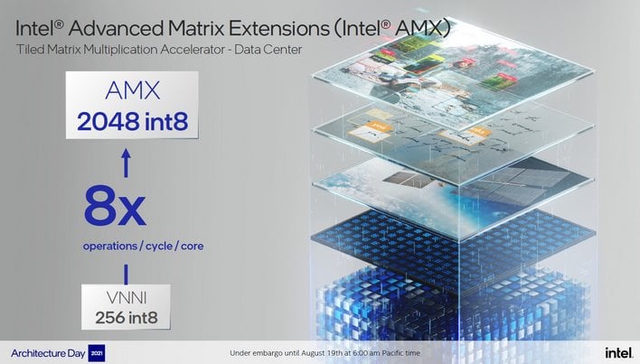
- Intel Advanced Matrix Extensions (AMX) – A new workload acceleration engine introduced in Sapphire Rapids that delivers massive speed-up to the tensor processing at the heart of deep learning algorithms. It can provide an increase in computing capabilities with 2K INT8 and 1K BFP16 operations per cycle. Using early Sapphire Rapids silicon, optimized internal matrix-multiply micro benchmarks run over 7x faster using new Intel AMX instruction set extensions compared to a version of the same micro benchmark using Intel AVX-512 VNNI instructions, delivering substantial performance gains across AI workloads for both training and inference
- Intel Data Streaming Accelerator (DSA) – Designed to offload the most common data movement tasks that cause the overhead seen in data center scale deployments. Intel DSA improves processing of these overhead tasks to deliver increased overall workload performance and can move data among CPU, memory and caches, as well as all attached memory, storage and network devices

In conjunction with the new cores and accelerators, Sapphire Rapids’ LLC (Last Level Cache) and memory subsystems will enable increased performance and flexibility. Up to 100MB of LLC can be shared across all cores and IP on Sapphire Rapids. And that massive cache will be fed by up to 4 memory controllers and 8 memory channels, with support for emerging DDR5 memory technology, next-gen Optane Persistent Memory 300, or HBM. We should also note that HBM configurations can be used in conjunction with DDR5 as well. HBM can be configured in 2 modes – Flat Mode, with flat memory regions for HBM and DRAM or a Caching Mode, where the HBM is fed by a DRAM backed cache.

Sapphire Rapids also offers improved multi-socket scaling, thanks to Intel Ultra Path Interconnect 2.0, or UPI 2.0. The processors will feature up to four x24 UPI links, operating at 16GT/s and implement a new up to 8 socket / 4 UPI topology, optimized for high performance applications.
Next generation Sapphire Rapids Xeon Scalable Processors are due to arrive early next year.
New Intel Infrastructure Processing Units (IPU) Are Inbound
Intel also announced a trio of new Infrastructure Processing Units, including its first ASIC IPU. This new crop of IPUs leverage a mix of Intel Xeon-D processor cores, Intel Agilex FPGAs and Intel Ethernet technologies – along with all of the associated IO and connectivity – to allow cloud and communication service providers to offload infrastructure tasks (like networking, storage and remote management) from CPUs, to ultimately reduce overhead and increase throughput. IPUs also enable the separation of infrastructure from tenant or guest software, so guests can fully control the CPU with their software, while service providers maintain control of the infrastructure and root-of-trust. IPUs can help enable diskless server architectures as well, to provide additional flexibility to service providers.
Intel’s new Oak Springs Canyon IPU features Intel Xeon-D cores, an Agilex FPGA, and dual 100 gigabit Ethernet network interfaces. It supports Intel’s Open vSwitch technology, and enables the offloading of network virtualization and storage functions, like NVMe over fabric and RoCE v2, to reduce CPU overhead. It offers a hardened crypto block to secure its network connections as well. Customers can customize the card using Intel’s Open FPGA Stack and it can be programmed using commonly used software environments, like the Data Plane or Storage Performance Development Kits, i.e. DPDK and SPDK.
Next up we have the Intel N6000 Acceleration Development Platform, codenamed Arrow Creek. Arrow Creek is a 100G SmartNIC designed for use with Intel Xeon-based servers. It features an Intel Agilex FPGA and Intel Ethernet 800 Series controller for high-performance 100 gigabit network acceleration. Arrow Creek targets Communication Service Providers (CoSPs) and allows them to offer flexible acceleration options for workloads like Juniper Contrail, OVS and SRv6.

Intel’s new ASIC IPU, codenamed Mount Evans, is the first product of its type from Intel. The company claims Mount Evans was architected and developed in cooperation with a top cloud service partner, and integrates features and technologies gleaned from developing multiple generations of FPGA-based SmartNICs.
Mount Evans features up to 16 Arm Neoverse N1 cores, with a dedicated compute cache and up to 3 memory channels. It has a dedicated management processor and a lookaside crypto and compression engine as well. The ASIC can support up to four host Xeons, with 200Gb/s of full duplex bandwidth between them.
Mount Evans reportedly offers a best-in-class programmable packet processing engine and a hardware accelerated NVMe storage interface, scaled up from Intel Optane technology, to emulate NVMe devices. Mount Evans also leverages Intel Quick Assist technology to aid in the deployment of advanced crypto and compression acceleration, and like its counterparts, it can be programmed using common software environments.
Xe-HPC-Based Ponte Vecchio: It’s Italian – It Must Be Good
Intel has been talking about Ponte Vecchio for quite a while. Ponte Vecchio is a Xe architecture-based GPU optimized for HPC and AI workloads, which will be a key component of the upcoming Aurora exascale super computer at the Argonne National Laboratory. Before we dive into Intel’s latest disclosures regarding Ponte Vecchio, however, we must first talk about Intel’s Xe-Core, or what the company calls the “compute building block of Xe HPC-based GPUs."
Each Xe-Core has 8 Vector Engines (512-bit per engine) and 8 Matrix Engines (4096-bit per engine), which Intel refers to as XMX, or Xe Matrix eXtensions. Each core offers 512B/clk of load / store bandwidth and 512K of L1 cache / shared local memory. The Vector Engine is capable of 256 FP32 or FP64 ops/clk, or 512 FP16 ops/clk. And the Matrix Engine is capable of 2048 TF32 operations per clock, 4096 FP16 or BF16 ops/clock, and 8192 INT8 ops/clock.

Over and above the single Xe-Core capabilities, Intel also outlined how Cores can be incorporated into Slices, and how Slices can be arranged into Stacks. Each Xe Slice features up to 16 Xe-Cores, with a total of up to 8MB of L1 cache. Each of those cores gets an adjacent Ray Tracing Unit, and the Slice gets a single Hardware Context Switch.

A Stack will consist of up to four slices, with a total of 64 Xe-Cores and associated IP (64 RTUs and 4 Hardware Contexts). A stack also incorporates the L2 cache, four HBM2e controllers, one Media Engine, and 8 Xe Links, for linking Stacks together. At this point, you can probably see where this is going, but we digress…
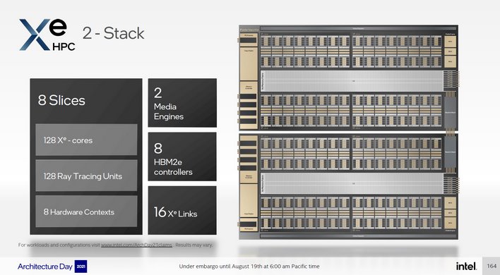
Xe Link is a high-speed, coherent GPU-to-GPU fabric, that handles load/store, bulk data transfer and semantics synchronization. With 8 Xe Links per Stack, up to 8 GPUs can be fully connected through an embedded switch, for what can ultimately be a massive amount of compute.

Which brings us to Ponte Vecchio. If ever there was a product designed to showcase as many bleeding-edge technologies as possible, it is this Intel product. Ponte Vecchio consist of over 100B transistors and leverages numerous tiles, is manufactured using 5 different process nodes and multiple foundries, linked together using EMIB, Foveros, and specialized tiles, on packages that required inventing new verification and qualification tools. Ponte Vecchio is ambitious as heck.

A Ponte Vecchio SoC features 47 active tiles; multiple Compute, Rambo cache, Base, HBM, Xe Link and EMIB tiles. In addition, there’s a Foveros layer (36um Bump Pitch) and specialized multi-tile packaging.

Ponte Vecchio’s Compute Tiles are manufactured on TSMC’s N5 node and feature 8 Xe-Cores, with 4MB of L1 cache. The Base Tile, which has an area of 640mm2, is built on Intel 7, and packs in 144MB of L2 cache, the PCIe Gen 5 and multi-die fabric interfaces, and EMIB. Then there’s the Xe-Link tile, which is built on TSMC’s N7 node, and offers 8 links per tile.

In addition to the fresh technical detail, Intel also revealed some initial performance data. A0 Ponte Vecchio silicon is reportedly offering >45 TFLOPS FP32 throughput, with >5TBps memory fabric bandwidth and >2TBps of connectivity bandwidth. Intel also showed a ResNet inference performance demo running at over 43,000 images per second and a ResNet training demo at over 3,400 images per second, which are big numbers at this early stage to say the least.
Intel Architecture Day 2021: The Wrap Up
Intel has been facing fierce competition on multiple fronts from numerous competitors over the last few years, with no sign of a respite in sight. With new leadership at the helm under the guide of the revered Pat Gelsinger and what appears to be a broad array of healthy, ambitious technologies coming down the pipeline, however, the company seems prepared to maintain its leadership position in multiple markets.Of course, we’ll have to wait and see how Intel executes on all of these lofty plans. For now, these latest disclosures will have to hold us over while we wait for October and the first Intel Innovation event in the Intel On Series (aka IDF 2.0). There is sure to be some fireworks at that event, so stay tuned.


