Haswell-E Debuts: Intel Core i7-5960X Processor Review
Haswell-E Explained
Haswell-E, and by extension the Core i7-5960X Extreme Edition, has a lot in common with 4th gen Intel Core processors based on the Haswell microarchitecture, which arrived mid-last year with the Core i7-4770K and other members of the processor family—Haswell-E is just bigger and badder. Because the fundamental architectures are so similar, we won’t be rehashing many of the details again here, but we would suggest checking out a few previous articles if you’d like more details regarding some of the tech employed in Haswell-E, like Intel’s Turbo Boost Technology 2.0, Smart Cache, Smart Response Technology, etc.
- Intel Core i7-4770K Review: Haswell Has Landed
- Intel's Haswell: Optimized For Mobility
- Z97 Motherboard Round Up: EVGA, MSI, Gigabyte
In our Core i7-4770K / Haswell launch article, we go in-depth on the Haswell microarchitecture and cover many details that are pertinent to today’s launch as well. Some additional architectural details are covered in our "Optimized For Mobility" piece and in on our Intel Z97 Motherboard Round-Up article, we cover many of the features available oin the X99 chipset, since the Z97 and X99 share a few similarities.
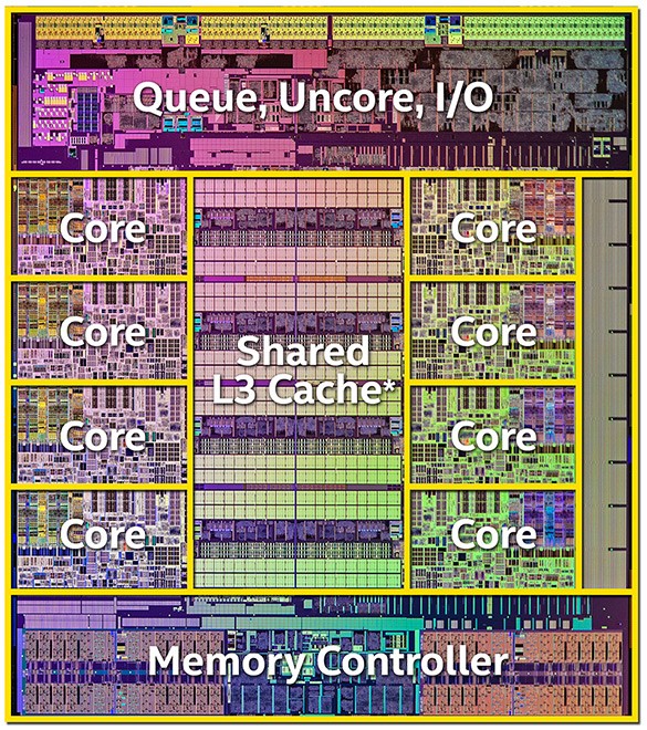
As we’ve mentioned, Haswell-E shares many of the same features of the original Haswell microarchitecture, but as the “E” denotes, Haswell-E is more extreme. What you see pictured above is a die map of a Haswell-E based Core i7-5960X Extreme Edition processor. The chip is manufactured using Intel’s advanced 22nm process node and features roughly 2.66 billion transistors. The die size is approximately 355.5mm2 (17.6 mm x 20.2 mm).
The initial batch of processors based on the Haswell-E microarchitecture will feature either 8 or 6 active execution cores that can each process two threads simultaneously courtesy of Intel’s Hyper-Threading technology, for support of a total of up to 16 threads. The actual execution cores are essentially identical to the original Haswell microarchitecture and support the same Intel AVX and AES instructions, along with SSE4.1, SSE4.2, and so on.
Haswell-E based processors like the Core i7-5960X Extreme Edition are designed for a new socket, LGA 2011 v3, and require a compatible motherboard built around the new X99 chipset (more on that later). The processors will support up to 20MB of shared L3 Intel Smart Cache, and feature integrated quad-channel memory controllers with official support for DDR4 memory at speeds up to 2133MHz, although higher speeds are possible through overclocking.
Haswell-E based processors also feature up to 40 integrated lanes of PCI Express connectivity that support the 8GT/s PCI Express 3.0 specification. We say “up to” in the previous sentence, because there is one Haswell-E based processor coming down the pipeline that features only 28 lanes.


Intel Core i7-5960X Extreme Edition Processor CPU-Z Details
The Intel Core i7-5960X Extreme Edition processor we’ll be featuring here today has a base clock frequency of 3GHz with a maximum Turbo frequency of 3.5GHz. It achieves those clocks using a BCLK of 100MHz (mistakenly labeled bus speed in the image above) and multipliers ranging from 30 to 35, although lower and higher multipliers are available with this unlocked processor. The chip sports 256K of L1 data cache (32K per core), 256K of L1 instruction cache (32K per core), and 2MB of L2 cache (256K per core). The Core i7-5960X Extreme Edition is also outfitted with 20MB of shared L3 cache, although lower-end variants of the chip will have 15MB (or potentially less).
The chip has a 140W TDP, which is slightly higher than the 130W of Ivy Bridge-E based processors and has an approximate .7v base input voltage, although that voltage will automatically scale upwards when higher multipliers are used, like when Turbo Boost frequencies kick in, for example.


