Intel Xeon W-3175X Review: Supercharged 28-Core Skylake-SP
Intel Xeon W-3175X - Unleashing The 28-Core Beast
In October of last year, when Intel officially unveiled its 9th Generation Core series processors, the company also took the opportunity to announce a semi-new breed of workstation processor, namely the Xeon W-3175X. Technically speaking, the architecture at the heart of the Xeon W-3175X isn’t new – the monstrous 28-core / 56-thread processor is based on Skylake-SP, just like the first wave of Xeon Scalable processors that were released in 2017. What Intel has done with the Xeon W-3175X, however, is selectivity bin the die and tweak and tune the power and turbo boost profiles to increase frequencies, and ultimately performance, versus earlier Skylake-SP parts. The Xeon W-3175X is also unlocked to allow for easier overclocking, like more mainstream "K" skus.
To help bring this ultra-powerful processor to market, Intel also enlisted the help of a couple of its partners to produce motherboards that could provide copious amounts of power, should users want to overclock the Xeon W-3175X. The ASUS ROG Dominus Extreme motherboard we tested the Xeon W-3175X with, for example, is packing 32 power phases and features dual 24-pin ATX, quad 8-pin EPS12V, and dual 6-pin 12V feeds to keep everything from the processor, to the memory, and the PCI Express slots fed with ample power when pushed well beyond stock.
Below is a quick breakdown of the Intel Xeon W-3175X’s main features and specifications. Take a peek at the speeds and feeds and then we’ll check out the hardware more closely and see how it performs in comparison to many of today’s top-end processors...
The Intel Xeon W-3175X is an extension of the Xeon W series, with higher clocks and unlocked multipliers. The processor features 28 physical cores with support for 56 threads, thanks to Intel’s HyperThreading (SMT) technology. The W-3175X’s base clock is 3.1GHz and its single-core Turbo frequency is 4.3GHz. In comparison, the Xeon Platinum 8180 28-core processor, which is based on the same architecture, has a base clock of 2.5GHz and max Turbo frequency of 3.8GHz.
As we’ve mentioned, the Xeon W-3175X is based on Skylake-SP, which is fundamentally similar to Skylake-X and the original Skylake microarchitectures. Because we’ve covered Skylake in all of its forms in the past, we’re not going to dig too deeply into them again here. If you would like more background, however, we do have a few articles to suggest. In our original coverage of the Intel Xeon Scalable series of processors, we discuss the intricacies of Skylake-SP and Skylake-X is detailed in our coverage of the Core i7-7900X. Our Intel Skylake Architecture Preview from IDF is worth a look as well.
There are some things about Skylake-SP we should reiterate, though. Like the Xeon Scalable Series, the Xeon W-3175X is manufactured using Intel’s 14nm process. With that in mind, packing 28 cores in a single, monolithic die and pushing frequencies and voltages upward is going to result in some hefty power requirements. The Xeon W-3175X has a 255W TDP, but as you’ll see a little later, power consumption can be significantly higher when overclocking.
The processor supports 6 memory channels (with standard RAS and ECC support), has 38.5MB of Intel Smart Cache, 48 integrated PCI Express 3.0 lanes (with an additional 20 coming by way of the companion C621 chipset), and it requires an LGA3647 socket.
Skylake-SP quadruples the size of the L2 cache versus older architectures, bringing it up to 1MB per core, but the size of the shared L3 cache reduced. In its entirety, however, there is still roughly the same amount of total cache -- the balance has just been shifted. Not only have the cache sizes changed, but how they are utilized has been changed as well.
Intel has previously employed an inclusive cache structure. With such a large L2 cache on Skylake-SP, however, an inclusive cache didn’t make sense anymore, because copies of the cache data would need to be maintained in multiple layers, which would effectively reduce the total amount of L3 available. And duplicating a large amount of L2 on a smaller L3 didn’t make any sense whatsoever. To increase the size of the L2 and simultaneously keep the L3 cache size larger, Intel would have had to sacrifice core count to keep die sizes in check, so the decision was made to move to a non-inclusive cache structure. This change results in a better hit-rate in the larger, lower-latency L2 cache, and a negligibly lower hit-rate on the smaller L3.
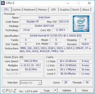
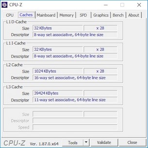
Getting back to the Intel Xeon W-3175X, here is a look at its CPU-Z details while idling, while under load, and with only a single core being utilized. The processor's all-turbo boost hit 3.8GHz with 1.04v. Single core boost tickled the 4.3GHz mark, but was difficult to capture due to constant frequency fluctuations. 4.1GHz – 4.2GHz clocks at about 1.1v were much more common. The cache breakdown is also represented here. As you can see, the processor has 64K (32K + 32K) of L1 per core, 1MB of L2 per core, and a total of 38.5MB of shared L3.
To help bring this ultra-powerful processor to market, Intel also enlisted the help of a couple of its partners to produce motherboards that could provide copious amounts of power, should users want to overclock the Xeon W-3175X. The ASUS ROG Dominus Extreme motherboard we tested the Xeon W-3175X with, for example, is packing 32 power phases and features dual 24-pin ATX, quad 8-pin EPS12V, and dual 6-pin 12V feeds to keep everything from the processor, to the memory, and the PCI Express slots fed with ample power when pushed well beyond stock.
Below is a quick breakdown of the Intel Xeon W-3175X’s main features and specifications. Take a peek at the speeds and feeds and then we’ll check out the hardware more closely and see how it performs in comparison to many of today’s top-end processors...
|
The Intel Xeon W-3175X is an extension of the Xeon W series, with higher clocks and unlocked multipliers. The processor features 28 physical cores with support for 56 threads, thanks to Intel’s HyperThreading (SMT) technology. The W-3175X’s base clock is 3.1GHz and its single-core Turbo frequency is 4.3GHz. In comparison, the Xeon Platinum 8180 28-core processor, which is based on the same architecture, has a base clock of 2.5GHz and max Turbo frequency of 3.8GHz.
As we’ve mentioned, the Xeon W-3175X is based on Skylake-SP, which is fundamentally similar to Skylake-X and the original Skylake microarchitectures. Because we’ve covered Skylake in all of its forms in the past, we’re not going to dig too deeply into them again here. If you would like more background, however, we do have a few articles to suggest. In our original coverage of the Intel Xeon Scalable series of processors, we discuss the intricacies of Skylake-SP and Skylake-X is detailed in our coverage of the Core i7-7900X. Our Intel Skylake Architecture Preview from IDF is worth a look as well.
There are some things about Skylake-SP we should reiterate, though. Like the Xeon Scalable Series, the Xeon W-3175X is manufactured using Intel’s 14nm process. With that in mind, packing 28 cores in a single, monolithic die and pushing frequencies and voltages upward is going to result in some hefty power requirements. The Xeon W-3175X has a 255W TDP, but as you’ll see a little later, power consumption can be significantly higher when overclocking.
The processor supports 6 memory channels (with standard RAS and ECC support), has 38.5MB of Intel Smart Cache, 48 integrated PCI Express 3.0 lanes (with an additional 20 coming by way of the companion C621 chipset), and it requires an LGA3647 socket.
Skylake-SP quadruples the size of the L2 cache versus older architectures, bringing it up to 1MB per core, but the size of the shared L3 cache reduced. In its entirety, however, there is still roughly the same amount of total cache -- the balance has just been shifted. Not only have the cache sizes changed, but how they are utilized has been changed as well.
Intel has previously employed an inclusive cache structure. With such a large L2 cache on Skylake-SP, however, an inclusive cache didn’t make sense anymore, because copies of the cache data would need to be maintained in multiple layers, which would effectively reduce the total amount of L3 available. And duplicating a large amount of L2 on a smaller L3 didn’t make any sense whatsoever. To increase the size of the L2 and simultaneously keep the L3 cache size larger, Intel would have had to sacrifice core count to keep die sizes in check, so the decision was made to move to a non-inclusive cache structure. This change results in a better hit-rate in the larger, lower-latency L2 cache, and a negligibly lower hit-rate on the smaller L3.
Intel Skylake-SP Mesh Architecture
Linking all of the cores, cache, and I/O in Skylake-SP is a mesh architecture that is different than the ring interconnect used in previous-gen processors. The mesh, in conjunction with the changes to the cache hierarchy, however, do alter the overall performance profile of the Skylake-SP (and Skylake-X) versus other architectures. As core counts and memory and I/O bandwidth increased, it became increasingly more difficult to maximize efficiency with a ring interconnect. A ring interconnect would require data to be sent across long stretches (relatively speaking) of the ring to reach its intended destination, for example. The new mesh architecture addresses this limitation by interconnecting on-chip elements in a more pervasive way, to ultimately increase the number of pathways and improve efficiency.Getting back to the Intel Xeon W-3175X, here is a look at its CPU-Z details while idling, while under load, and with only a single core being utilized. The processor's all-turbo boost hit 3.8GHz with 1.04v. Single core boost tickled the 4.3GHz mark, but was difficult to capture due to constant frequency fluctuations. 4.1GHz – 4.2GHz clocks at about 1.1v were much more common. The cache breakdown is also represented here. As you can see, the processor has 64K (32K + 32K) of L1 per core, 1MB of L2 per core, and a total of 38.5MB of shared L3.


