NVIDIA's GeForce 7 Update: Introducing the 7900 GTX, 7900 GT & 7600 GT
The GeForce 7900 GTX & 7900 GT
![]()
A quick glance at the architecture of the new GeForce 7900 series products shows that little has changed in terms of the general block diagram. That's not to say, however, that the G71 chip itself isn't radically different from its predecessor, the G70, which became known as the GeForce 7800 GTX. Although parts of the G71 have been re-architected for efficiency and transistor saving, the GeForce 7900 does borrow heavily from the G70.
|
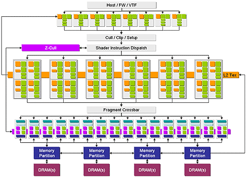
GeForce 7900 Series GPU Block Diagram
90nm - 278M transistors
For the GeForce 7900 we're still looking at a 24 pixel pipeline machine that comes equipped with 16 Raster Ops and 8;) with 8 vertex shader units and 16 ROPs. The GPU also still derives its memory buffer bandwidth over a 256-bit interface as well. This new GeForce 7 series GPU is built on TSMC's new 90nm fabrication process, which is definitely leading edge by today's standards, but perhaps just not "bleeding edge" where it's oh-so easy to get cut trying to catch a falling knife, so to speak. We're sure 65nm is on the horizon for the major graphics vendors as well, but for now 90nm process geometries are more than adequate for bringing these highly complex Graphics Processor cores to market.
with 8 vertex shader units and 16 ROPs. The GPU also still derives its memory buffer bandwidth over a 256-bit interface as well. This new GeForce 7 series GPU is built on TSMC's new 90nm fabrication process, which is definitely leading edge by today's standards, but perhaps just not "bleeding edge" where it's oh-so easy to get cut trying to catch a falling knife, so to speak. We're sure 65nm is on the horizon for the major graphics vendors as well, but for now 90nm process geometries are more than adequate for bringing these highly complex Graphics Processor cores to market.
Speaking of which, the new GeForce 7900 series has actually lightened its load a bit by dropping a few transistors as a result of design optimizations and tweaks, made to the Shader Engines, ROPs, SLI interface, and Z-Cull logic, in this spin of the chip. The ROPs specifically have been re-architected to improve blending performance, while other portions of the chip were tweaked for efficiency. The result is that the new GeForce 7900 series has a 278 million transistor count versus roughly 302 million transistors in the GeForce 7800 GTX. Looking comparatively at the die size versus ATI's new Radeon X1900 series product, you'll also note that the GeForce 7900 series is significantly smaller, 196mm2 versus 352mm2 to be exact. This was part of NVIDIA's approach on this architecture refresh, one we feel that should certainly bode very well for them, from an overall cost standpoint.
The GeForce 7900 still only has 24 pixel shader engines, which almost sounds a bit meager when you consider the Radeon X1900 XT series comes equipped with 48 pixel shaders but those 48 shader engines are only supported by 16 Raster Operators in the X1900 and balanced resources in any architecture, are always critical. Adding in additional Raster Ops along with Shader Engines would most definitely blow out die size even more, so instead NVIDIA chose to drive the manufacturing process to 90nm, which offers obvious gains in both clock speeds, die size, thermals and power consumption. When you consider how well the GeForce 7800 performs with its 430 - 450MHz core, it doesn't take a rocket scientist to know that a 200MHz increase in clock speed and a bit more head-room on that memory interface speed, could likely be all that's needed to take the current architecture to the next level. And imagine what 90nm could do for costs, with the same clock speeds. It becomes clear that NVIDIA may have played this one masterfully, as long as TSMC's process can churn out the volume.
|
![]()
;)
;)
;)
;)
;)
;)
NVIDIA GeForce 7900 GTX:
24-Pixel Shader Units / 8 Vertex Shader Units / 16-ROPs / 256-Bit Memory Interface
650MHz Core / 700MHz Vertex / 800MHz (1.6GHz DDR) Memory (256MB) - Pricing $499 - $649
As you can see, the new GeForce 7900 GTX looks just like the 512MB 7800 GTX it usurps as NVIDIA's flagship desktop part. A quick visual inspection did not reveal any differences in the PCB design, and both cards share the same dual-slot cooler with heat-pipes, which first appeared on NVIDIA's high-end Quadro workstation graphics cards. There are some major differences between the 7900 GTX and 7800 GTX, though. First, the 7900 GTX now features a pair of dual-link DVI outputs, thanks to the two dual-links TMDSs within the G71 GPU. As we mentioned earlier, the GPU is also manufactured on a more advanced 90nm processes which allowed NVIDIA to crank the core clock speed way up on the 7900 GTX. The reference spec calls for a GPU clocked at 650MHz, with a 700MHz geometry clock. And the card's 512MB frame buffer is clocked at 800MHz (1.6GHz DDR), which is actually a bit lower than the 512MB GeForce 7800 GTX. The GeForce 7900 GTX also features a new 7-pin HDTV output, as opposed to the 9-pin output on previous cards, that supports direct connection of S-Video cables or an HD Component output adapter. NVIDIA expects pricing on the 7900 GTX to fall within the $499 to $649 range, depending on the specific card configuration and bundle offered by their board partners. That's a wide range, for sure, but in-line with what the market has supported the past couple of product cycles.
The GeForce 7900 GTX also fully supports NVIDIA's relatively new Quad-SLI technology, which links four GPUs together for increased performance and potentially better image quality when using SLIAA -- up to 32X AA in fact. At CES we saw what was essentially four GeForce 7800 GTX cards running in Dell's high-end XPS Renegade rig, but at a recent event, NVIDIA was showing of Quad-SLI GeForce 7900 rigs from a handful of strategic partners, including Alienware, Falcon and Voodoo. We hope to bring you a comprehensive look at a Quad-SLI rig in the near future and plan to go more in-depth then. What we can tell you now is that NVIDIA made true quad-SLI possible by designing a 48-lane, 3-port PCI Express switch, which offers full PCI Express x16 bandwidth to all four GPUs when installed on an nForce 4 SLIX16 chipset based motherboard. And to fully harness the power of four GPUs, NVIDIA is introducing a new rendering mode called "AFR of SFR". To put it simply, with AFR of SFR rendering, alternate frames are then slit in two parts with each GPU only working on roughly half, or every other frame.
![]()
;)
;)
;)
;)
;)
;)
NVIDIA GeForce 7900 GT:
24-Pixel Shader Units / 8 Vertex Shader Units / 16-ROPs / 256-Bit Memory Interface
450MHz Core / 470MHz Vertex / 660MHz (1.32GHz DDR) Memory (256MB) - MSRP $299 - $399
We suspect this next addition to the GeForce 7 series line-up will be very popular amongst the Enthusiast and Gaming communities. The new GeForce 7900 GT is essentially a scaled-down 7900 GTX, that differs from the new flagship in only a few ways. The 7900 GT and 7900 GTX share the exact same GPU with dual dual-link DVI outputs, but it is clocked at a more conservative 450MHz as per the reference spec. The 7900 GT also sports a 256MB frame buffer clocked at 1.32GHz, half that of the GTX, a smaller, less elaborate PCB, and a much smaller, single-slot copper cooler. The specifications put the 7900 GT just above the 256MB 7800 GTX in NVIDIA's product line-up, but the pricing scale for the 7900 GT is much more attractive. NVIDIA expects cards to be available for prices between $299 to $399, depending on the frame buffer configuration, clock speeds, and bundles offered by their partners.


