Intel's Evolution Of The Transistor Innovation Is A Fun Trip Down Silicon Memory Lane
We tend to take for granted that our PCs will turn on and the silicon inside them will dutifully crunch through whatever tasks we ask, be it video encoding, playing games, or even just watching a YouTube video. The underlying technology has come a long way to make all this possible, and crucially it has taken decades of continual transistor innovation to get us where we are today, and where we want to go tomorrow. Reflecting on that, Intel posted a rather interesting video that visualizes the evolution of the transistor.
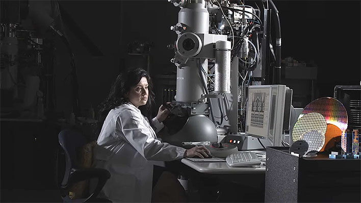
It's narrated by Marisa Ahmad, whose job title is Technology Leadership Marketing Process and Manufacturing. Early in her career, Ahmad developed an appreciation for transistors from operating a scanning electronic microscope, which makes visible what would otherwise be far to small to be seen by the naked eyeball.
At its basic level, a transistor is a "simple little switch" in which energy is applied to a gate to turn off or on a current flow to the channel underneath. The design is of course more complex, and over time the distance those electrons flowed have gotten shorter. Engineers have also added more layers and materials to the mix, and employed difference techniques in the overall design.
The general idea is the create faster, smaller transistors that consume less power, and those goals are quite the challenge. However, they're all crucial to developing more sophisticated CPUs with ever-increasing capabilities.
Intel's video above takes you through some of the bigger milestones and innovations along the way, like creating a Shallow Trench Isolation (STI) technique in 1995 to further shrink the wide insulating gaps that were required between each transistor.
It's interesting to look back as Intel forges ahead while attempting to maintain Moore's Law. Today's chips contain billions of transistors, and that number is not going to shrink. The transistors themselves will, but as Intel points, that alone is not enough to deliver continued leaps in performance.

"Today, we are continuing to evolve our roadmap to one that showcases new levels of innovation and moving to an accelerated pace to enable an annual cadence of process improvements.
With our new Intel 4 and Intel 3 technologies, we are fully embracing EUV lithography, which involves a highly complex optical system of lenses and mirrors that focuses a 13.5 nm wavelength of light to print incredibly small features on silicon. This is a vast improvement over prior technology that used light at a wavelength of 193nm," Intel explains.
Intel's also looking ahead to its Intel 20A process, which ushers in the angstrom era with RibbonFET and a backside power delivery technology it is calling PowerVIA. We'll have to wait and see how it all plays out in the years to come. In the meantime, enjoy the trip down silicon memory lane.