JEDEC Updates High Bandwidth Memory (HBM) Standard To 24GB Per Stack At Blistering 307GBps
JEDEC announced an update to the the JESD235 memory standard that deals with the second generation of high bandwidth memory (HBM). This update brings two key feature enhancements to the standard. First, it raises the capacity limit for each device to 24GB, and it also raises the speed threshold to 307GB/s.
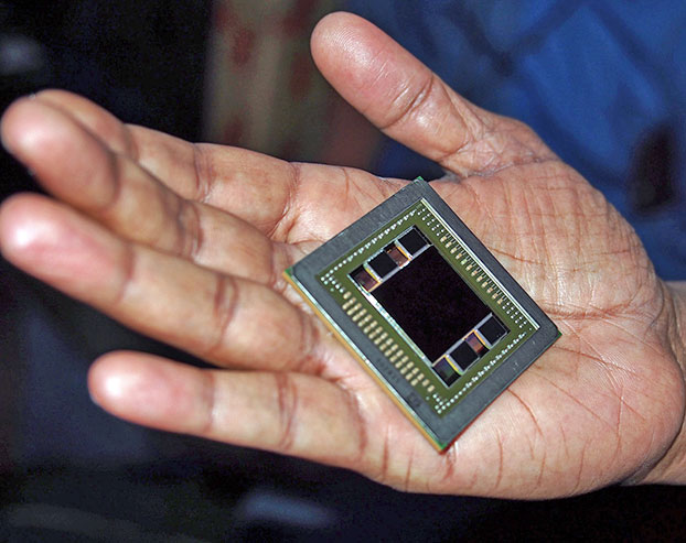
If you are unfamiliar with HBM memory, you should know that it was first introduced in 2013 as an ultra fast alternative to more traditional DDR RAM. HBM differs significantly from DDR RAM, in that it operates at relatively slow clock speeds but over an enormous bus that is typically 1024-bit wide. This creates a plethora of bandwidth, and the original HBM standard was able to attain speeds of 128GB/s. This was doubled with the second generation of HBM memory to 256GB/s, and now rises to 307GB/s.
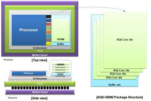
Equally as important is the increase in capacity, which has been an ongoing problem for companies implementing HBM designs. HBM memory chips are organized into four groups with memory chips stacked on top of each other. This has limited the total capacity of HBM over the years, and the original HBM standard maxed out at 4GB. HBM2 improved this by enabling stacks of up to eight memory modules, which pushed the limit up to 8GB. AMD's has been making the most of this technology, and the company's Radeon RX Vega graphics cards all come with 8GB of memory, but this has also held AMD back somewhat. NVIDIA has competing products that contain as much as 11GB of GDDR5X RAM.
The new JEDEC JESD235B standard will now make it possible for AMD to push the amount of RAM up on its graphics cards further, giving it an even footing to compete with NVIDIA on memory capacity. It will likely be sometime before we see new products that use this updated memory standard appear on the market though.