New AMD Triple-Core Phenom And Roadmap Details
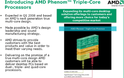
As a follow-up to our coverage of AMD's new triple-core announcement from last night, we have some additional details for you regarding the product's high-level architecutre as well as forward-looking product roadmap information.
AMD Triple-Core Phenom Architecture
Since the time of our initial coverage yesterday, officials at AMD have confirmed that indeed the new triple-core Phenom is based on an identical die, that is employed in quad-core Phenoms due out later this year. As you'll note, these new triple cores still have their own discrete per-core 512KB L2 cache, as well as a 2MB shared L3 cache, again which is identical to the quad-core architecture.
AMD's strategy to leverage quad-core devices that fall out of the manufacturing process as tested but still have three fully functional cores, could well prove to be a significant advantagefor the company, in terms of mitigating yield loss and its associated impact on profit margins.
AMD notes that triple-core Phenoms will ship in Q1 '08 and as we see, "Toliman", which is the core code-name for the triple-core Phenom, will also have a dual-core counterpart in that time frame, code-named "Kuma". Beyond that we see AMD has DDR3 support in their future Deneb and Propus cores, with follow-on triple and dual-core offerings Heka and Regor, which are based on those those later quad-core architectures as well.


