NVIDIA's 7nm Ampere A100 Beast Machine Learning GPU Launched With DGX A100 AI Supercomputer
According to NVIDIA, its Ampere-based A100 GPU is already in full production and shipping to customers, and it is claiming that the A100 represents the single largest generational uplift in GPU performance in its history. Given the specs, we have no reason to doubt the company.

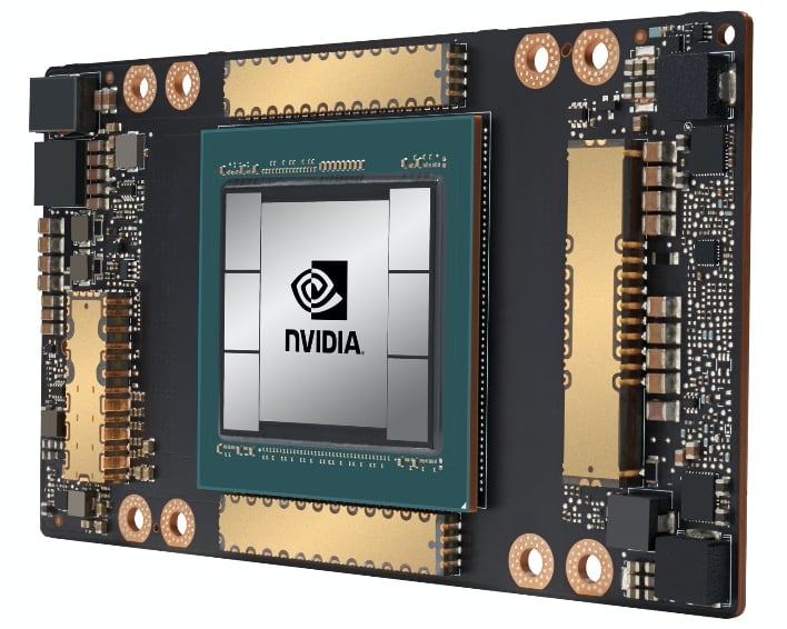
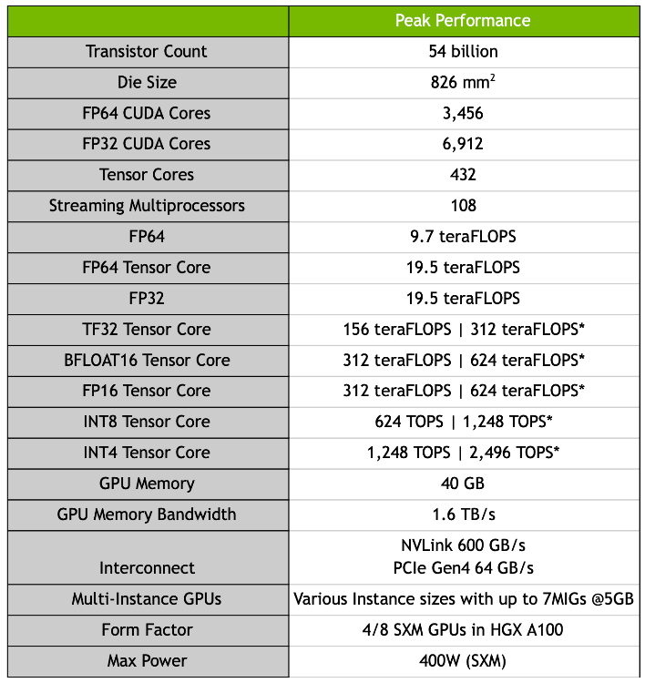
The A100 features a whopping 54 billion transistors, which definitely allows it to take the crown as the world's largest processor built on 7nm tech. There are a total of 6,912 FP32 CUDA cores, 432 Tensor cores, and 108 SMs. Onboard is 40GB of HBM2e memory with maximum memory bandwidth of 1.6TB/sec. FP32 compute comes in at a staggering 19.5 TLFLOPs, compared to 16.4 TFLOPs for Tesla V100s. FP64 compute stands at 9.7 TFLOPs, compared to 8.2 TFLOPs for Tesla V100s. In addition, its Tensor Cores employ FP32 precision that allows for a 20x uplift in AI performance. When it comes to FP64 performance, these Tensor Cores also provide a 2.5x performance boost, compared to its predecessor, Volta, with respect to HPC (High Performance Compute) applications.
Some other Ampere-specific features include Multi-instance GPU, aka MIG, which allows an A100 GPU to be sliced up into up to seven discrete instances. That way, the raw power of the chip can be provisioned for multiple discrete specialized workloads. Ampere also integrates a third-generation NVLink design, which doubles the performance of interconnect between multiple GPUs for improved scaling.
“NVIDIA A100 GPU is a 20x AI performance leap and an end-to-end machine learning accelerator — from data analytics to training to inference," said NVIDIA founder and CEO Jensen Huang. "For the first time, scale-up and scale-out workloads can be accelerated on one platform. NVIDIA A100 will simultaneously boost throughput and drive down the cost of data centers.”
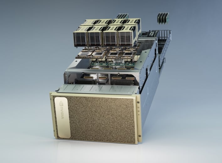
Those A100 GPUs will also make their way into NVIDIA's third-generation DGX AI supercomputer, with 5 PetaFLOPs of AI performance. Jensen gave us an early "taste" of DGX A100 when he pulled a freshly-baked rig out of his personal home oven on Tuesday. At the time, he declared it to be “the world’s largest graphics card," but unfortunately its targeted duties aren't for gaming.
The DGX A100 has a total of eight A100 GPUs, along with 320GB of memory (12.4TB per second in bandwidth). The system is also equipped with Mellanox HDR 200Gbps interconnects. As we mentioned before, each A100 GPU can support up to 7 instances, which means that with 8 GPUs onboard, the DGX A100 can support a grand total of 56 instances to attack the workload at hand.

However, NVIDIA is also thinking beyond just the DGX A100, and has announced the development of the DGX SuperPOD, which combines the power of 140 DGX A100 systems linked using the aforementioned Mellanox interconnects. Together, you're looking at 700 petaflops of AI compute power, which can be used for anything from medical research to helping analyze COVID-19, as we've seen with the Folding@Home project.
NVIDIA looks to be getting off to a strong start with Ampere and the A100, but we're of course also looking forward to seeing what the company has in store for the enthusiast market. It's been over 18 months since NVIDIA launched its Turing architecture with the GeForce RTX 20 family, and expectations for the GeForce RTX 30 family are incredibly high.