Ampere Is Big But NVIDIA's GH100 Hopper Could Be The Biggest GPU Ever By Far
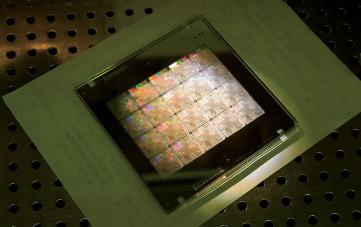
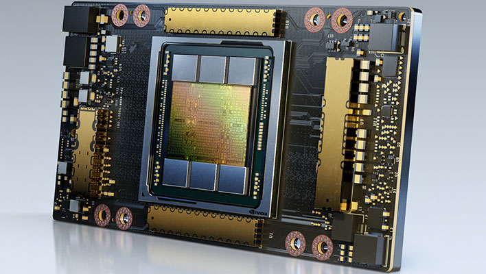
NVIDIA sells a huge parallel processor called A100. This is based on a gigantic Ampere-architecture processor called GA100, an 826 mm² chip. That makes it expensive to manufacture and power-thirsty to operate, but by all accounts it delivers on performance. It's actually the second of such massive monolithic processors from the company, with the first being the Volta-based GV100; that one was 815 mm².
Up next in GeForce land we're expecting to meet Lady Ada Lovelace, but at the ultra-high-end enterprise computing end of the scale, the next up is Grace Hopper. Named after the US Navy Rear Admiral who was one of the inventors of the compiler-linker structure that we use for most code today, NVIDIA's Hopper GPU will supposedly be the next in its series of massively-parallel compute processors for datacenters.
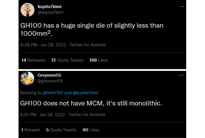
If we're to believe leakers Greymon55 and kopite7kimi, Hopper will be far and away the largest monolithic GPU ever made. Prior reports had indicated that Hopper would take a multi-chip module (MCM) approach, combining multiple smaller dice into a single package much like AMD's Instinct MI200. According to these leakers, Hopper "GH100" will be monolithic, larger than GA100, and possibly in the realm of 900-1000 mm².
The thing is, current lithography equipment has a reticle limit of about 858 mm². That means that the largest die that can be etched without moving the reticle is about 850 mm² in area. To create a larger chip would require an expensive and time-consuming cross-reticle stitching process where the processor has to be etched in stages.
On Twitter, Dr. Ian Cutress—who we've talked process tech with in the past—expressed similar dubiousness about the veracity of the leak. He comments that if NVIDIA were going to fabricate a processor that large, they might be treading on others companies' patents, and those companies are not likely to license that technology. He also notes that a die that large would be exceptionally prone to defects, and would bin poorly. According to Cutress, the ultimate result is unlikely to be a superior product to what can be achieved using a single reticle.
To kopite7kimi's credit, he walked back his earlier claim slightly after it gained some pushback. He states firmly that GH100 will be larger than GA100, but he isn't actually sure about the die size. Simply being larger than the biggest Ampere makes it an enormous GPU already, but it remains to be seen just how much larger it will actually be.
NVIDIA is expected to announce Hopper officially at its Graphics Technology Conference in March, so we'll probably know more by then.