SanDisk Pushes Memory Smaller With 19nm Technology
45nm? Old. 32nm? Close, but no cigar. 19nm? That's the stuff. We're just
kidding around about 45nm process technology being "so last year," but
in reality, things truly are evolving really quickly in the CPU
universe. And maybe even faster in the memory universe. SanDisk is
obviously a major player in the latter, and they just announced a new
19-nanometer manufacturing technology, which is listed as the world's
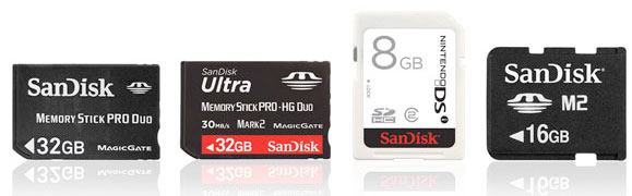
smallest, most advanced process node. The 19nm 64-gigabit X2 memory chip
is the smallest NAND memory chip in the world, with volume production
slated for 2H 2011.
SanDisk will sample its 19nm 64Gb X2 device this quarter, and once they hit mass production, the company will also add 3-bits-per-cell (X3) products fabricated with the 19nm process technology to its product lineup. What's this mean for you? More memory packed into tighter spaces, in other words, good things for your future gadget buys!
SanDisk will sample its 19nm 64Gb X2 device this quarter, and once they hit mass production, the company will also add 3-bits-per-cell (X3) products fabricated with the 19nm process technology to its product lineup. What's this mean for you? More memory packed into tighter spaces, in other words, good things for your future gadget buys!
SanDisk Announces 19-Nanometer Manufacturing Technology—World’s Smallest, Most Advanced Process Node
* Industry-leading 19nm 64-gigabit X2 memory chip; smallest NAND flash memory chip in the world
* Volume production scheduled for the second half of 2011
MILPITAS, Calif.--(BUSINESS WIRE)--SanDisk Corporation (NASDAQ:SNDK), the global leader in flash memory cards, today announced a 64-gigabit (Gb), 2-bits-per-cell (X2) based monolithic chip made on 19-nanometer (nm) technology, the most advanced memory process technology node in the world. This latest technology enables SanDisk to produce embedded and removable storage devices with the high capacities and small form factors used in mobile phones, tablet computers and other devices.
“We are excited to introduce the world’s smallest and lowest-cost NAND flash chips based on industry-leading 19nm process technology in our ongoing collaboration with our manufacturing partner Toshiba”
SanDisk will sample its 19nm 64Gb X2 device this quarter and expects to begin high-volume production in the second half of 2011. At that time, SanDisk will also add 3-bits-per-cell (X3) products fabricated with the 19nm process technology to its product lineup.
“We are excited to introduce the world’s smallest and lowest-cost NAND flash chips based on industry-leading 19nm process technology in our ongoing collaboration with our manufacturing partner Toshiba,” said Yoram Cedar, executive vice president and chief technology officer, SanDisk. “Products based on this technology are designed to enable new applications, form factors and consumer experience that will continue to drive the flash industry to new heights.”
The 19nm memory die uses the most sophisticated flash memory technology node to date, including advanced process innovations and cell-design solutions. SanDisk’s All-Bit-Line (ABL) architecture with proprietary programming algorithms and multi-level data storage management schemes help yield multi-level cell (MLC) NAND flash memory chips that do not sacrifice performance or reliability.