TSMC 3nm Chip Production On Track For Late 2022 With Huge Power Efficiency Gains

Even though there is a shortage of silicon (relative to rabid demand), the pace of technology has now slowed. Just ask Taiwan Semiconductor Manufacturing Company (TSMC), one of the biggest players in the semiconductor space with clients such as Apple, AMD, Intel, and others. It's been producing 5-nanometer chips in volume since last year (and is building an advanced 5nm chip fab in Arizona), and is on track to enter the volume production phase for 3nm in the second half of 2022.
The funny thing about nanometer designations is that smaller nodes and how a company goes about labeling them are the not the end-all-be-all in semiconductors. Intel, for example, would argue that its 10nm node is roughly on par with AMD's 7nm node. That is a whole discussion in and of itself. Along those lines, however, TSMC says its 3nm node will be the most advanced technology in the world when it arrives in volume next year.
Part of the boast is related to N3's significant improvement in power efficiency, compared to TSMC's N5 node.

Source: TSMC
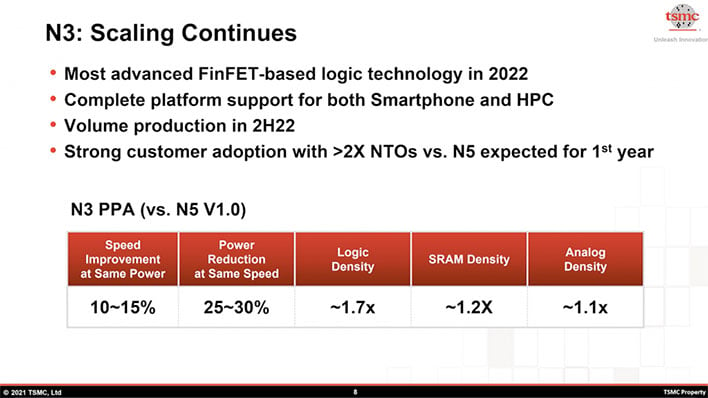
"Relying on the proven FinFET transistor architecture for the best performance, power efficiency, and cost effectiveness, N3 will offer up to 15 percent speed gain or consume up to 30 percent less power than N5, and provide up to 70 percent logic density gain," TSMC said.
To be clear, N3 is a generational leap, or a full-node advanced from N5, just as N5 was a full-node advance for N7. TSMC has been working on it for years—the company stated in 2019 that development for its N3 node was "going well with early customers engaged." TSMC did not drop any names, but it is entirely possible AMD was one of those 'engaged' customers.
AMD's current generation Zen 3 processor are built on a 7nm node from TSMC, and its Zen 4 processors will see a transition to 5nm when they arrive in the first half of 2022, with DDR5 support in tow (and PCI Express 5.0 support on the server side, but not on consumer CPUs). While nothing has been confirmed further out than that, it is conceivable (and rumored) that Zen 5 will leverage TSMC's 3nm node.
Rumor has it Zen 5 will also adopt a heterogeneous design similar to what Intel is doing with Alder Lake—pairing high performance cores with power efficient cores in the same package. Arm has been doing this in the mobile space for a long time now with its big.LITTLE branding, and the hybrid approach is now headed to mainstream x86 computing as well.
Source: TSMC
As for TSMC's 3nm node, however, the foundry is touting complete platform support for smartphones and high performance computing (HPC) applications. Paving the way for better performance and power efficiency, the N3 node will deliver a 1.7x increase in logic density and a 1.2x jump in SRAM density compared to N5, TSMC says.
Interestingly, TSMC senior vice president of research and development, Dr. Yuh Jier Mii, said during the company's 2021 Online Technology Symposium that the company has seen double the number of tape-outs in N3's first year compared to N5. This is the stage prior to wrapping up a design and sending it in for production.
it will be a bit before there are actual consumer products leveraging TSMC's N3 node, but it will be interesting to see what exactly they entail when they do arrive, either by the end of 2022 or early 2023.