NVIDIA GeForce GTX 1080 Performance Review: Pascal, The New King
Pascal Architecture Overview
As we’ve mentioned, the GPU powering the GeForce GTX 1080 is based on NVIDIA’s Pascal architecture. Pascal is the follow-up to Maxwell, which is used on NVIDIA’s GeForce GTX 900-series of discrete graphics cards and mobile GPUs.
The specific Pascal-derived GPU at the heart of the GTX 1080 is codenamed the GP104. The GP100, which was revealed a few weeks back on the Tesla P100, is the “big” version of Pascal that uses HBM2 memory and will presumably show up in the consumer space somewhere down the road (maybe). The GP104 is a scaled-down version of that chip targeted at gamers, which uses standard GDDR5 or newer GDDR5X memory. Note: this is the GeForce GTX 1080, not a GTX 1080 Ti.
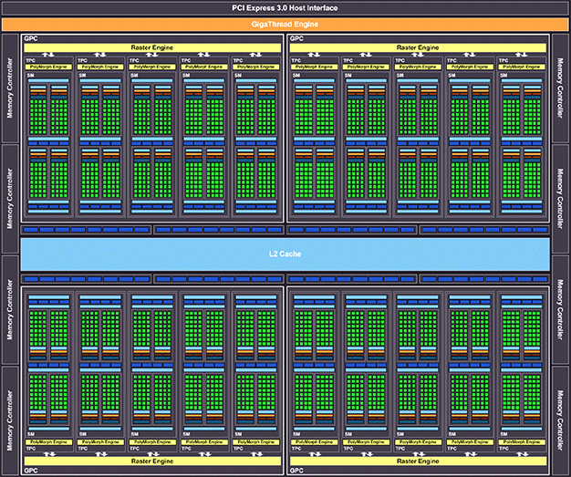
NVIDIA GP104 Block Diagram

NVIDIA GP104 Block Diagram
The GP104 is manufactured using TSMC’s 16nm FinFET process. The GPU is comprised of roughly 7.2 billion transistors and has a die size measuring 314mm2. That’s significantly smaller than the 398mm2 area of the Maxwell-based GM204 used on the GTX 980, which featured 5.2 billion transistors – 2 billion fewer than the GP104.
In its full implementation, the GP104 features 20 streaming multiprocessors (SM) with a total of 2560, single-precision CUDA cores, arranged in 4 graphics processing clusters (GPC).

A GP104 SM
Each GPC includes a dedicated raster engine and five SMs with 128 CUDA cores, eight texture units, 256 KB of register file capacity – double the previous generation, a 96 KB shared memory unit, and 48 KB of total L1 cache. There is 2MB of L2 cache on the chip, and a total of 160 texture units. Each SM is also outfitted with a PolyMorph Engine that handles vertex fetch, tessellation, viewport transformation, vertex attribute setup, and perspective correction. It's also in the PolyMorph Engine that a new unit enables a feature called Simultaneous Multi-Projection, which we'll talk about later.
The GeForce GTX 1080 also features eight 32-bit memory controllers, for 256-bits in total. Linked to each 32-bit memory controller are eight ROPs, for a total of 64, and 256 KB of that aforementioned L2 cache. Along with the newly configured memory controller, the GeForce GTX 1080 leverages newly-released GDDR5X memory (the upcoming 1070 will use standard GDDR5). Peak bandwidth per-pin with traditional GDDR5 memory is 8Gbps. With GDDR5X, however, bandwidth per pin is increased up to 10Gbps - 14Gb/s.
To achieve the effective 10Gbps speed on the GeForce GTX 1080's memory interface, NVIDIA had to redesign the I/O circuit architecture and pay special attention to detail on the channel between the GPU and individual memory dies, to ensure clean signaling. NVIDIA notes that the redesign will also help future products that may use GDDR5 memory, thanks to the improved data integrity across the memory circuitry.
In addition to the new GPU arrangement and increased register space, Pascal also offers a number of new features over Maxwell, which we’ll dive into next.


