NVIDIA GeForce GTX 480: GF100 Has Landed
NVIDIA GF100 Architecture
![]()
The Fermi GPU architecture, that is the foundation of the GF100 GPU powering the GeForce GTX 480, features over 3 billion transistors and is produced using TSMC's 40nm processes. If you remember, AMD's RV870, which is used in the ATI Radeon HD 5870, is comprised of roughly 2.15 billion transistors and is also manufactured at 40nm. Fermi will be outfitted with more than double the number of cores as the current GT200, 512 in total, but as it is implemented on the GeForce GTX 480 only 480 shader processors are exposed. The GPU will offer 8x the peak double-precision compute performance as its predecessor, and Fermi will be the first GPU architecture to support ECC. ECC support will allow Fermi to compensate for soft error rate (SER) issues that can be problematic in larger bleeding-edge IC designs and also potentially allow it to scale to higher densities. The GPU will also be execute C++ code.

GF100 High-Level Block Diagram
The GF100 is a significant architectural change from previous GPU architectures. In the block diagram above, the first major changes made to GF100 become evident. In each GPC cluster--there are four in the diagram--newly designed Raster and Polymorph Engines are present. We'll provide more detail on these GPU segments a little later, but having these engines present in each GPC segment essentially allows each one to function as a full GPU. The design was implemented to allow for better geometry performance scalability, through a parallel implementation of geometry processing units. According to NVIDIA, the end result in an 8X improvement in geometry performance over the GT200. Segmenting the GPU in this way also allows for multiple levels of scalability, either at the GPC or streaming multi-processor unit level, etc.
Each GF100 GPU features 512 CUDA cores, 16 geometry units, 4 raster units, 64 texture units, 48 ROPs, and a 384-bit GDDR5 memory interface. If you're keeping count, the GT200 features 240 CUDA cores, 42 ROPs, and 60 texture units. Remember though, only 480 cores are exposed on the GeForce GTX 480, 448 on the GTX 470. The geometry and raster units, as they are implemented in GF100, are not in the GT200 GPU. The GT200 also features a wider 512-bit memory interface, but the need for such a wide interface is somewhat negated in GF100 because the GPU uses GDDR5 memory which effectively offers double the bandwidth of GDDR3, clock for clock.
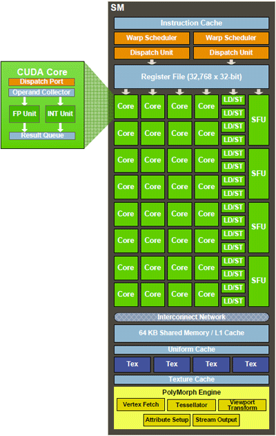
If we drill down a little deeper, each SM core in each GPC is comprised of 32 CUDA cores, with 48/16KB of shared memory (3 x that of GT200), 16/48KB of L1 (there is no L1 cache on GT200), 4 texture units, and 1 PolyMorph Engine. In addition to the actual units, we should point out that improvements have also been made over the previous generation for 32-bit integer operations performance and for full IEEE-754 2008 FMA support. The increase in cache size and the addition of L1 cache were designed to keep as much data resident on the GPU as possible, without having to go off-chip to external memory.

The L1 cache is used for register spilling, stack ops, and global loads and stores, while the L2 cache is for vertex, SM, texture, and ROP data. According to NVIDIA, the GF100's cache structure offers many benefits over GT200 in gaming applications, including faster texture filtering and more efficient processing of physics and ray tracing, in addition to greater texture coverage and generally better overall compute performance.

The PolyMorph and Raster Engines in the GPU perform very different tasks, but in the end result in greater parallelism in the GPU. The PolyMorph Engines are used for world space processing, while the Raster Engines are for screen space processing. There are a total of 16 polymorph engines placed before each SM. They allow work to be distributed across the chip, but there is also intelligent logic in place designed to keep the data in order. Communications happen between the units to ensure the data arrives in DRAM in the correct order and all of the data is kept on die, thanks to the chip's cache structure. Synchronization is handled at the thread scheduling level. The four independent Raster Engines serve the geometry shaders running in each GPC and the cache architecture is used to pass data from stage to stage in the pipeline. We're also told that the GF100 offers 10x faster context switching over the GT200, which further enhances performance when compute and graphics modes are both being utilized.


